Features: · 1.5GHz Operation with 250mV Differential Output Swing
· 2ps(RMS) (max) Random Jitter
· AC Specifications Guaranteed for 150mV Differential Input
· Signal Inputs Accept Any Differential Signaling Standard
· LVDS Outputs for Clock or High-Speed Data
· High-Level Input Fail-Safe Detection (MAX9390)
· Low-Level Input Fail-Safe Detection (MAX9391)
· +3.0V to +3.6V Supply Voltage Range
· LVCMOS/LVTTL Logic Inputs Control Signal RoutingApplication·High-Speed Telecom/Datacom Equipment
·Central-Office Backplane Clock Distribution
·DSLAM
·Protection Switching
·Fault-Tolerant SystemsPinout Specifications
VCC to GND......................................................-0.3V to +4.1V
IN_ _, IN_ _, OUT_ _, OUT_ _, EN_ _,
_SEL_ to GND.........................................-0.3V to (VCC + 0.3V)
IN_ _ to IN_ _ .................................................................±3V
Short-Circuit Duration (OUT_ _, OUT_ _) ..............Continuous
Continuous Power Dissipation (TA = +70°C)
32-Pin QFP (derate 13.1mW/°C
above +70°C).........................................................1047mW
32-Pin 5mm x 5mm Thin QFN (derate 21.3mW/°C
above +70°C).........................................................1702mW
Junction-to-Ambient Thermal Resistance in Still Air
32-Pin QFP..........................................................+76.4°C/W
32-Pin 5mm x 5mm Thin QFN.................................+47°C/W
Junction-to-Case Thermal Resistance
32-Pin 5mm x 5mm Thin QFN....................................+2°C/W
Operating Temperature Range .................-40°C to +85°C
Junction Temperature..............................................+150°C
Storage Temperature Range ..................-65°C to +150°C
ESD Protection (Human Body Model)
(IN_ _, IN_ _, OUT_ _, OUT_ _, EN_ _, SEL_ _) ..........±2kV
Soldering Temperature (10s) .................................+300°C
Stresses beyond those listed under "Absolute Maximum Ratings" may cause permanent damage to the device. These are stress ratings only, and functional operation of the device at these or any other conditions beyond those indicated in the operational sections of the specifications is not implied. Exposure to absolute maximum rating conditions for extended periods may affect device reliability.
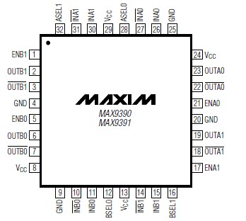
DescriptionThe MAX9390/MAX9391 dual 2 x 2 crosspoint switches perform high-speed, low-power, and low-noise signal distribution. The MAX9390/MAX9391 multiplex one of two differential input pairs to either or both low-voltage differential signaling (LVDS) outputs for each channel. Independent enable inputs turn on or turn off each differential output pair.
Four LVCMOS/LVTTL logic inputs of MAX9390 (two per channel) control the internal connections between inputs and outputs. This flexibility allows for the following configurations: 2 x 2 crosspoint switch, 2:1 mux, 1:2 splitter, or dual repeater. This makes the MAX9390/MAX9391 ideal for protection switching in fault-tolerant systems, loopback switching for diagnostics, fanout buffering for clock/data distribution, and signal regeneration.
Fail-safe circuitry forces the outputs to a differential lowcondition for undriven inputs or when the commonmode voltage exceeds the specified range. The MAX9390 provides high-level input fail-safe detection for LVDS, HSTL, and other GND-referenced differential inputs. The MAX9391 provides low-level input fail-safe detection for LVPECL, CML, and other VCC-referenced differential inputs.
Ultra-low 82ps(P-P) (max) pseudorandom bit sequence (PRBS) jitter of MAX9390 ensures reliable communications in highspeed links that are highly sensitive to timing error, especially those incorporating clock-and-data recovery, or serializers and deserializers. The high-speed switching performance guarantees 1.5GHz operation and less than 65ps (max) skew between channels.
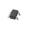
LVDS inputs and outputs are compatible with the TIA/EIA-644 LVDS standard. The LVDS outputs drive 100 loads. The MAX9390/MAX9391 are offered in a 32-pin TQFP and 5mm x 5mm thin QFN package with exposed paddle and operate over the extended temperature range (-40°C to +85°C).
Also refer to the MAX9392/MAX9393 with flow-through pinout.

 MAX9390 Data Sheet


