MAX9389

Features: · 310ps Propagation Delay· Guaranteed 2.7GHz Operating Frequency· 0.3psRMS Random Jitter· <30ps Output-to-Output Skew· -2.375V to -5.5V Supplies for Differential LVECL/ECL· +2.375V to +5.5V Supplies for Differential LVPECL/PECL· Outputs Low for Open Inputs· Dual Output Buffers· >2k...

product image

MAX9389 Picture
SeekIC No. : 004412668 Detail

MAX9389: Features: · 310ps Propagation Delay· Guaranteed 2.7GHz Operating Frequency· 0.3psRMS Random Jitter· <30ps Output-to-Output Skew· -2.375V to -5.5V Supplies for Differential LVECL/ECL· +2.375V to +...

floor Price/Ceiling Price

Part Number:
MAX9389
Supply Ability:
5000

Price Break

  • Qty
  • 1~5000
  • Unit Price
  • Negotiable
  • Processing time
  • 15 Days
Total Cost: $ 0.00

SeekIC Buyer Protection PLUS - newly updated for 2013!

  • Escrow Protection.
  • Guaranteed refunds.
  • Secure payments.
  • Learn more >>

Month Sales

268 Transactions

Rating

evaluate  (4.8 stars)

Upload time: 2024/11/27

Payment Methods

All payment methods are secure and covered by SeekIC Buyer Protection PLUS.

Notice: When you place an order, your payment is made to SeekIC and not to your seller. SeekIC only pays the seller after confirming you have received your order. We will also never share your payment details with your seller.
Product Details

Description


Features:

· 310ps Propagation Delay
· Guaranteed 2.7GHz Operating Frequency
· 0.3psRMS Random Jitter
· <30ps Output-to-Output Skew
· -2.375V to -5.5V Supplies for Differential LVECL/ECL
· +2.375V to +5.5V Supplies for Differential LVPECL/PECL
· Outputs Low for Open Inputs
· Dual Output Buffers
· >2kV ESD Protection (Human Body Model)


Application

High-Speed Telecom and Datacom Applications
Central-Office Backplane Clock Distribution
DSLAM/DLC


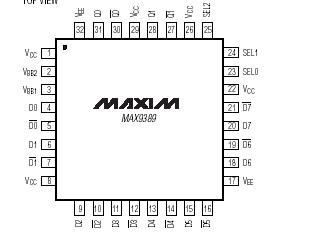
Pinout

  Connection Diagram


Specifications

VCC - VEE ...............................................................-0.3V to +6.0V
Inputs (D_, D_, SEL_) to VEE ......................-0.3V to (VCC + 0.3V)
D_ to D_.............................................................................±3.0V
Continuous Output Current ................................................50mA
Surge Output Current.......................................................100mA
VBB_ Sink/Source Current ..............................................±600µA
Continuous Power Dissipation (TA = +70)
   32-Lead TQFP (derate 13.1mW/above +70) ........1047mW
      JA in Still Air............................................................+76/W
      JC ..........................................................................+25/W
   32-Lead QFN (derate 21.3mW/ above +70) ........1702mW
      JA in Still Air............................................................+47/W
      JC ............................................................................+2/W
Operating Temperature Range ............................-40 to +85
Junction Temperature.......................................................+150
Storage Temperature Range ..............................-65 to +150
ESD Protection
Human Body Model (D_, D_, Q_, Q_, SEL_, VBB_) .............2kV
Soldering Temperature (10s) ...........................................+300

Stresses beyond those listed under "Absolute Maximum Ratings" may cause permanent damage to the device. These are stress ratings only, and functional operation of the device at these or any other conditions beyond those indicated in the operational sections of the specifications is not implied. Exposure to absolute maximum rating conditions for extended periods may affect device reliability.


Description

The MAX9389 is a fully differential, high-speed, low-jitter, 8-to-1 ECL/PECL multiplexer (mux) with dual output buffers. The device is designed for clock and data distribution applications, and features extremely low propagation
delay (310ps typ) and output-to-output skew (30ps max).

Three single-ended select inputs, SEL0, SEL1, and SEL2, control the mux function. The mux select inputs of MAX9389 are compatible with ECL/PECL logic, and are internally referenced to the on-chip reference output (VBB1, VBB2), nominally VCC - 1.425V. The select inputs accept signals between VCC and VEE. Internal pulldowns to VEE ensure
a low default condition if the select inputs are left open.

The differential inputs D_, D_ of MAX9389 can be configured to accept a single-ended signal when the unused complementary
input is connected to the on-chip reference output (VBB1, VBB2). All the differential inputs of MAX9389 have internal bias and clamping circuits that ensure a low output state when the inputs are left open.

The MAX9389 operates with a wide supply range VCC - VEE of 2.375V to 5.5V. The device is offered in 32-pin TQFP and thin QFN packages, and operates over the -40 to +85 extended temperature range.


Customers Who Bought This Item Also Bought

Margin,quality,low-cost products with low minimum orders. Secure your online payments with SeekIC Buyer Protection.
Isolators
Cables, Wires
Line Protection, Backups
Crystals and Oscillators
Static Control, ESD, Clean Room Products
View more