Features: 318ps (typ) Propagation Delay
>2.7GHz Toggle Frequency
0.3ps(RMS) Random Jitter
<14ps (max) at +25°C Output-to-Output Skew
(MAX9387)
-2.375V to -5.5V Supplies for Differential LVECL/ECL
+2.375V to +5.5V Supplies for Differenti LVPECL/PECL
Outputs Low for Open Inputs
Dual Output Buffers (MAX9387)
Pin Compatible with MC100EP57 (MAX9388EUP)
>2kV ESD Protection (Human Body Model)ApplicationHigh-Speed Telecom and Datacom Applications
Central Office Backplane Clock Distribution
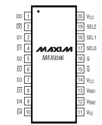
DSLAM/DLCPinout Specifications
Vcc - VEE..............................................................-0.3V to +6.0V
Inputs (D_, D_, SEL_) to VEE ....................-0.3V to (Vcc + 0.3V)
D_ to D_ ..........................................................................±3.0V
Continuous Output Current ..............................................50mA
Surge Output Current......................................................100mA
VBB_ Sink/Source Current .............................................±600A
Continuous Power Dissipation (TA = +70°C)
20-Lead TSSOP (derate 11.0mW/°C above +70°C) ....880mW
JA in Still Air ..............................................................+91°C/W
JC .............................................................................+20°C/W
24-Lead TSSOP (derate 12.2mW/°C above +70°C) .....976mW
JA in Still Air ..............................................................+82°C/W
JC .............................................................................+15°C/W
20-Lead QSOP (derate 9.1mW/°C above +70°C) .......727mW
JA in Still Air ............................................................+110°C/W
JC .............................................................................+34°C/W
24-Lead QSOP (derate 9.5mW/°C above +70°C) .......762mW
JA in Still Air ............................................................+105°C/W
JC ............................................................................+34°C/W
Operating Temperature Range .......................-40°C to +85°C
Junction Temperature....................................................+150°C
Storage Temperature Range .........................-65°C to +150°C
ESD Protection
Human Body Model (D_, D_, Q_, Q_, SEL_, VBB_) .............2kV
Lead Temperature (soldering, 10s) ..............................+300°C
Stresses beyond those listed under "Absolute Maximum Ratings" may cause permanent damage to the device. These are stress ratings only, and functional operation of the device at these or any other conditions beyond those indicated in the operational sections of the specifications is not implied. Exposure to absolute maximum rating conditions for extended periods may affect device reliability.
DescriptionThe MAX9386/MAX9387/MAX9388 are fully differential, high-speed, low-jitter ECL/PECL multiplexers (muxes) with output buffer(s). The devices are designed for clock-and-data distribution applications, and feature extremely low propagation delays (318ps, typ) and output- to-output skews (3.9ps, typ). The MAX9386 is a 5:1 mux with a single output buffer. The MAX9387 is a 5:1 mux with dual output buffers, and is intended for use in redundant systems. The MAX9388 is a 4:1 mux with a single output buffer, and is pin compatible with the MC100EP57.
Three single-ended select inputs, SEL0, SEL1, and SEL2, control the mux function on the MAX9386/ MAX9387. The MAX9388 has two select inputs, SEL0 and SEL1. The mux select inputs are compatible with ECL/PECL logic, and are internally referenced to the on-chip output VBB, nominally Vcc - 1.425V. The select inputs of MAX9388 accept signals between Vcc and VEE. Internal pulldowns to VEE ensure a low-default condition if the select inputs are left open.
The differential inputs D_, D_ can be configured to accept a single-ended signal when the unused complementary input is connected to the on-chip reference output VBB. All the differential inputs have internal bias and clamping circuits that ensure low-default output states when the inputs are left open.
The MAX9386/MAX9387/MAX9388 operate with a wide supply range |VCC - VEE| of 2.375V to 5.5V. The MAX9386/MAX9388 are offered in 20-pin TSSOP and QSOP packages. The MAX9387 is offered in 24-pin TSSOP and QSOP packages.

 MAX9388 Data Sheet


