Features: · 1.2ps (RMS) Maximum Random Jitter
· 300mV Differential Output at 1.0GHz
· 900ps Propagation Delay
· Selectable Divide-by-1 or Divide-by-2 Frequency Outputs
· Multiplexed 2:1 Input Function
· LVECL Operation from VEE = -2.375V to -3.8V
· LVPECL Operation from VCC = +2.375V to +3.8V
· ESD Protection: > 2kV Human Body ModelApplication·Precision Clock Distribution
·Low-Jitter Data Repeaters
·Central-Office Backplane Clock Distribution
·DSLAM Backplane
·Base Stations
·ATEPinout Specifications
VCC to VEE.............................................................................4.1V
Inputs and Outputs to VEE..........................-0.3V to (VCC + 0.3V)
Differential Input Magnitude.............Lower of (VCC - VEE) and 3V
Continuous Output Current ................................................50mA
Surge Output Current........................................................100mA
VBB Sink/Source Current ...............................................±0.65mA
Continuous Power Dissipation (TA = +70°C)
Single-Layer PC Board
52-Pin TQFP (derate 15.4mW/°C above +70°C)......1230.8mW
68-Lead QFN (derate 27.8mW/°C above +70°C) ....2222.2mW
Multilayer PC Board
52-Pin TQFP (derate 19.1mW/°C above +70°C)......1529.6mW
68-Lead QFN (derate 38.5mW/°C above +70°C) ...3076.9mW
Junction-to-Ambient Thermal Resistance in Still Air
Single-Layer PC Board
52-Pin TQFP................................................................+65°C/W
68-Lead QFN ..............................................................+36°C/W
Multilayer PC Board
52-Pin TQFP.............................................................+52.3°C/W
68-Lead QFN .............................................................+26°C/W
Junction-to-Ambient Thermal Resistance with 500 LFPM Airflow
Single-Layer PC Board
52-Pin TQFP................................................................+50°C/W
68-Lead QFN .............................................................+27°C/W
Multilayer PC Board
52-Pin TQFP................................................................+40°C/W
68-Lead QFN .............................................................+20°C/W
Junction-to-Case Thermal Resistance
52-Pin TQFP.............................................................+12.9°C/W
68-Lead QFN ...............................................................+2°C/W
Operating Temperature Range ......................-40°C to +85°C
Junction Temperature...................................................+150°C
Storage Temperature Range .......................-65°C to +150°C
ESD Protection
Human Body Model (Q_ _, Q_ _, CLK_SEL,
FSEL_, CLK_, CLK_, MR, VBB) ...........................................±2kV
Soldering Temperature (10s) ......................................+300°C
Stresses beyond those listed under "Absolute Maximum Ratings" may cause permanent damage to the device. These are stress ratings only, and functional operation of the device at these or any other conditions beyond those indicated in the operational sections of the specifications is not implied. Exposure to absolute maximum rating conditions for extended periods may affect device reliability.
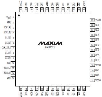
DescriptionThe MAX9322 low-skew 1:15 differential clock driver reproduces or divides one of two differential input clocks at 15 differential outputs. An input multiplexer selects from one of two input clocks with input switching frequency in exc ss of 1.0GHz. The 15 outputs are arranged in four banks with 2, 3, 4, and 6 outputs, respectively. Each output bank of MAX9322 is individually programmable to provide a divide-by-1 or divide-by-2 frequency function.
The MAX9322 operates in LVPECL systems with a +2.375V to +3.8V supply or in LVECL systems with a -2.375V to -3.8V supply. A VBB reference output provides compatibility with single-ended clock input signals and a master reset input provides a simultaneous reset on all outputs.
The MAX9322 is available in 52-pin TQFP and 68-pin QFN packages and is specified for operation over -40°C to +85°C. For 1:10 clock drivers, refer to the MAX9311/MAX9313 data sheet. For 1:5 clock drivers, refer to the MAX9316 data sheet .

 MAX9322 Data Sheet


