MAX9320A

Features: Improved Second Source of the MC10LVEP11 (MAX9320) +2.25V to +3.8V Differential HSTL/LVPECL Operation -2.25V to -3.8V LVECL Operation Low 22mA (typ) Supply Current 20ps (typ) Part-to-Part Skew 6ps (typ) Output-to-Output Skew 208ps (typ) Propagation Delay Minimum 300mV Output at 3GHz Out...

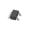
product image

MAX9320A Picture
SeekIC No. : 004412640 Detail

MAX9320A: Features: Improved Second Source of the MC10LVEP11 (MAX9320) +2.25V to +3.8V Differential HSTL/LVPECL Operation -2.25V to -3.8V LVECL Operation Low 22mA (typ) Supply Current 20ps (typ) Part-to-Part ...

floor Price/Ceiling Price

Part Number:
MAX9320A
Supply Ability:
5000

Price Break

  • Qty
  • 1~5000
  • Unit Price
  • Negotiable
  • Processing time
  • 15 Days
Total Cost: $ 0.00

SeekIC Buyer Protection PLUS - newly updated for 2013!

  • Escrow Protection.
  • Guaranteed refunds.
  • Secure payments.
  • Learn more >>

Month Sales

268 Transactions

Rating

evaluate  (4.8 stars)

Upload time: 2024/11/27

Payment Methods

All payment methods are secure and covered by SeekIC Buyer Protection PLUS.

Notice: When you place an order, your payment is made to SeekIC and not to your seller. SeekIC only pays the seller after confirming you have received your order. We will also never share your payment details with your seller.
Product Details

Description


Features:

 Improved Second Source of the MC10LVEP11 (MAX9320)
+2.25V to +3.8V Differential HSTL/LVPECL Operation
-2.25V to -3.8V LVECL Operation
Low 22mA (typ) Supply Current
20ps (typ) Part-to-Part Skew
6ps (typ) Output-to-Output Skew
208ps (typ) Propagation Delay
Minimum 300mV Output at 3GHz
Outputs Low for Open Input
ESD Protection >2kV (Human Body Model)
Available in Thermally Enhanced Exposed-Pad SO Package


Application

Precision Clock Distribution
Low-Jitter Data Repeater
Protection Switching


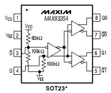
Pinout

  Connection Diagram


Specifications

VCC to VEE ..........................................................................+4.1V
D or D .................................................. VEE - 0.3V to VCC + 0.3V
D to D ................................................................................±3.0V
Continuous Output Current.................................................50mA
Surge Output Current........................................................100mA
Junction-to-Ambient Thermal Resistance in Still Air
   8-Pin SOT23.............................................................+112°C/W
   8-Pin TSSOP.............................................................+221°C/W
   8-Pin SO...................................................................+170°C/W
Junction-to-Ambient Thermal Resistance with 500
LFPM Airflow
   8-Pin SOT23...............................................................+78°C/W
   8-Pin TSSOP.............................................................+155°C/W
   8-Pin SO.....................................................................+99°C/W
Junction-to-Case Thermal Resistance
   8-Pin SOT23...............................................................+80°C/W
   8-Pin TSSOP...............................................................+39°C/W
   8-Pin SO.....................................................................+40°C/W
Operating Temperature Range ...........................-40°C to +85°C
Junction Temperature......................................................+150°C
Storage Temperature Range.............................-65°C to +150°C
ESD Protection
   Human Body Model (D, D , Q_, Q_ )......................................>2kV
Soldering Temperature (10s)...........................................+300°C
Stresses beyond those listed under "Absolute Maximum Ratings" may cause permanent damage to the device. These are stress ratings only, and functional operation of the device at these or any other conditions beyond those indicated in the operational sections of the specifications is not implied. Exposure to absolute maximum rating conditions for extended periods may affect device reliability.


Description

The MAX9320/MAX9320A are low-skew, 1-to-2 differential drivers designed for clock and data distribution. The input is reproduced at two differential outputs. The differential input can be adapted to accept single-ended inputs by applying an external reference voltage.

The MAX9320/MAX9320A feature ultra-low propagation delay (208ps), part-to-part skew (20ps), and output-to-output skew (6ps) with 30mA maximum supply current, making these devices ideal for clock distribution. For interfacing to differential HSTL and LVPECL signals, these devices operate over a +2.25V to +3.8V supply range, allowing high-performance clock or data distrib-ution in systems with a nominal +2.5V or +3.3V supply. For differential LVECL operation, these devices operate from a -2.25V to -3.8V supply.

The pinout is the only difference between the MAX9320 and MAX9320A. Multiple pinouts are provided to simplify routing across a backplane to either side of a double-sided board.

These MAX9320A are offered in space-saving 8-pin SOT23* and industry-standard TSSOP* and SO packages.


Customers Who Bought This Item Also Bought

Margin,quality,low-cost products with low minimum orders. Secure your online payments with SeekIC Buyer Protection.
Batteries, Chargers, Holders
Potentiometers, Variable Resistors
Semiconductor Modules
Connectors, Interconnects
Hardware, Fasteners, Accessories
View more