Maximum Operating Temperature
:
Package / Case
:
Packaging
:
Supply Voltage - Min
: 3 V
Output Logic Level
: LVECL, LVPECL
Supply Voltage - Max
: 3.8 V
Features: Guaranteed 400mV Differential Output at 1.5GHz
Selectable Single-Ended or Differential Input
130ps (max) Part-to-Part Skew at +25°C
20ps Output-to-Output Skew
365ps Propagation Delay
Synchronous Output Enable/Disable
On-Chip Reference for Single-Ended Inputs
Input Biased to Low when Open
Pin Compatible with MC100EL14ApplicationPrecision Clock Distribution
Low-Jitter Data Repeaters
Data and Clock Drivers and Buffers
Central-Office Backplane Clock Distribution
DSLAM Backplane
Base Stations
ATEPinout Specifications
VCC- VEE...............................................................................6.0V
Single-Ended Inputs (SCLK, SEL, EN , CLK, CLK )
For VCC- V EE 4.2V.................................VEE- 0.3V to VCC+ 0.3V
For VCC- V EE> 4.2V..................................VEE- 4.2V to VCC+ 0.3V
CLK to CLK .........................................................................±3.0V
Continuous Output Current.................................................50mA
Surge Output Current........................................................100mA
VBBSink/Source Current..................................................±0.65mA
Continuous Power Dissipation (TA= +70°C)
Single-Layer PC Board
20-Pin Wide SO (derate 10mW/°C above +70°C)..............800mW
Junction-to-Ambient Thermal Resistance in Still Air
Single-Layer PC Board
20-Pin Wide SO............................................................+100°C/W
Junction-to-Ambient Thermal Resistance with
500LFPM Airflow
Single-Layer PC Board
20-Pin Wide SO...............................................................+58°C/W
Junction-to-Case Thermal Resistance
20-Pin Wide SO...............................................................+20°C/W
Operating Temperature Range...............................-40°C to +85°C
Junction Temperature..........................................................+150°C
Storage Temperature Range.................................-65°C to +150°C
ESD Protection
Human Body Model (Inputs and Outputs)..................................2kV
Lead Temperature (soldering, 10s).....................................+300°C
Stresses beyond those listed under "Absolute Maximum Ratings" may cause permanent damage to the device. These are stress ratings only, and functional operation of the device at these or any other conditions beyond those indicated in the operational sections of the specifications is not implied. Exposure to absolute maximum rating conditions for extended periods may affect device reliability.
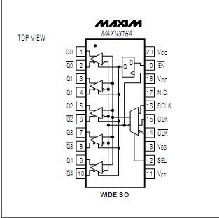
DescriptionThe MAX9316AEWP is a low-skew, 1-to-5 differential driver designed for clock and data distribution. This device allows selection between two inputs: one differential and one single ended. The selected input of MAX9316AEWP is reproduced at five differential outputs. The differential input can be adapted to accept a single-ended input by connecting the on-chip VBBsupply to one input as a reference voltage.
The MAX9316AEWP features low output-to-output skew (20ps), making it ideal for clock and data distribution across a backplane or board. For interfacing to differential HSTL and (LV)PECL signals, this device operates over a 3.0V to 5.5V supply range, allowing high-performance clock or data distribution in systems with a nominal 3.3V or 5.0V supply. For differential (LV)ECL operation, this MAX9316AEWP operates with a -3.0V to -5.5V supply. The MAX9316A is offered in a 20-pin wide SO package.

 MAX9316AEWP Data Sheet


