MAX9316A

Features: Guaranteed 400mV Differential Output at 1.5GHz Selectable Single-Ended or Differential Input 130ps (max) Part-to-Part Skew at +25°C 20ps Output-to-Output Skew 365ps Propagation Delay Synchronous Output Enable/Disable On-Chip Reference for Single-Ended Inputs Input Biased to Low when Op...

product image

MAX9316A Picture
SeekIC No. : 004412634 Detail

MAX9316A: Features: Guaranteed 400mV Differential Output at 1.5GHz Selectable Single-Ended or Differential Input 130ps (max) Part-to-Part Skew at +25°C 20ps Output-to-Output Skew 365ps Propagation Delay Syn...

floor Price/Ceiling Price

Part Number:
MAX9316A
Supply Ability:
5000

Price Break

  • Qty
  • 1~5000
  • Unit Price
  • Negotiable
  • Processing time
  • 15 Days
Total Cost: $ 0.00

SeekIC Buyer Protection PLUS - newly updated for 2013!

  • Escrow Protection.
  • Guaranteed refunds.
  • Secure payments.
  • Learn more >>

Month Sales

268 Transactions

Rating

evaluate  (4.8 stars)

Upload time: 2024/11/27

Payment Methods

All payment methods are secure and covered by SeekIC Buyer Protection PLUS.

Notice: When you place an order, your payment is made to SeekIC and not to your seller. SeekIC only pays the seller after confirming you have received your order. We will also never share your payment details with your seller.
Product Details

Description


Features:

Guaranteed 400mV Differential Output at 1.5GHz
Selectable Single-Ended or Differential Input
130ps (max) Part-to-Part Skew at +25°C
20ps Output-to-Output Skew
365ps Propagation Delay
Synchronous Output Enable/Disable
On-Chip Reference for Single-Ended Inputs
Input Biased to Low when Open
Pin Compatible with MC100EL14


Application

Precision Clock Distribution
Low-Jitter Data Repeaters
Data and Clock Drivers and Buffers
Central-Office Backplane Clock Distribution
DSLAM Backplane
Base Stations
ATE


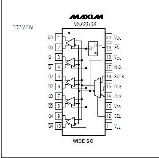
Pinout

  Connection Diagram


Specifications

VCC- VEE...............................................................................6.0V
Single-Ended Inputs (SCLK, SEL, EN , CLK, CLK )
For VCC- V EE 4.2V.................................VEE- 0.3V to VCC+ 0.3V
For VCC- V EE> 4.2V..................................VEE- 4.2V to VCC+ 0.3V
CLK to CLK .........................................................................±3.0V
Continuous Output Current.................................................50mA
Surge Output Current........................................................100mA
VBBSink/Source Current..................................................±0.65mA
Continuous Power Dissipation (TA= +70°C)
Single-Layer PC Board
20-Pin Wide SO (derate 10mW/°C above +70°C)..............800mW
Junction-to-Ambient Thermal Resistance in Still Air
Single-Layer PC Board
20-Pin Wide SO............................................................+100°C/W
Junction-to-Ambient Thermal Resistance with
500LFPM Airflow
Single-Layer PC Board
20-Pin Wide SO...............................................................+58°C/W
Junction-to-Case Thermal Resistance
20-Pin Wide SO...............................................................+20°C/W
Operating Temperature Range...............................-40°C to +85°C
Junction Temperature..........................................................+150°C
Storage Temperature Range.................................-65°C to +150°C
ESD Protection
Human Body Model (Inputs and Outputs)..................................2kV
Lead Temperature (soldering, 10s).....................................+300°C


Stresses beyond those listed under "Absolute Maximum Ratings" may cause permanent damage to the device. These are stress ratings only, and functional operation of the device at these or any other conditions beyond those indicated in the operational sections of the specifications is not implied. Exposure to absolute maximum rating conditions for extended periods may affect device reliability.


Description

The MAX9316A is a low-skew, 1-to-5 differential driver designed for clock and data distribution. This device allows selection between two inputs: one differential and one single ended. The selected input is reproduced at five differential outputs. The differential input of MAX9316A can be adapted to accept a single-ended input by connecting the on-chip VBBsupply to one input as a reference voltage.

The MAX9316A features low output-to-output skew (20ps), making it ideal for clock and data distribution across a backplane or board. For interfacing to differential HSTL and (LV)PECL signals, this MAX9316A operates over a 3.0V to 5.5V supply range, allowing high-performance clock or data distribution in systems with a nominal 3.3V or 5.0V supply. For differential (LV)ECL operation, this device operates with a -3.0V to -5.5V supply. The MAX9316A is offered in a 20-pin wide SO package.


Customers Who Bought This Item Also Bought

Margin,quality,low-cost products with low minimum orders. Secure your online payments with SeekIC Buyer Protection.
Discrete Semiconductor Products
Power Supplies - External/Internal (Off-Board)
Computers, Office - Components, Accessories
Line Protection, Backups
View more