Features: ` Programmable ±4%, ±2%, or OFF Spread-Spectrum Output for Reduced EMI
` Programmable DC-Balanced or Non-DC-Balanced Modes
` DC Balance Allows AC-Coupling for Wider Input Common-Mode Voltage Range
` Spread Spectrum Operates in DC-Balanced or Non-DC-Balanced Mode
` / 4 Deskew by Oversampling (MAX9242/MAX9244)
` 16MHz-to-34MHz (DC-Balanced) and 20MHz-to-40MHz (Non-DC-Balanced) Operation (MAX9242/MAX9244)
` 6MHz-to-18MHz (DC-Balanced) and 8MHz-to-20MHz (Non-DC-Balanced) Operation (MAX9246)
` Rising-Edge (MAX9242) or Falling-Edge (MAX9244/MAX9246) Output Strobe
` High-Impedance Outputs when PWRDWN is Low Allow Output Busing
` Fail-Safe Inputs in Non-DC-Balanced Mode
` Separate Output Supply Allows Interface to +1.8V,+2.5V, +3.3V, and +5V Logic
` LVDS Inputs Meet ISO 10605 ESD Protection at ±30kV Air-Gap Discharge and ±6kV Contact Discharge
` LVDS Inputs Meet IEC 61000-4-2 Level 4 ESD Protection at ±15kV Air-Gap Discharge and ±8kV Contact Discharge
` LVDS Inputs Conform to ANSI TIA/EIA-644 Standard
` +3.3V Main Power SupplyApplicationAutomotive Navigation Systems
Automotive DVD Entertainment Systems
Digital Copiers
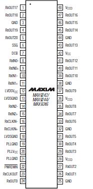
Laser PrintersPinout Specifications
(All voltages referenced to GND.)
VCC, LVDSVCC, PLLVCC .......................................-0.5V to +4.0V
VCCO....................................................................-0.5V to +6.0V
RxIN_, RxCLKIN_ .................................................-0.5V to +4.0V
PWRDWN ............................................................-0.5V to +6.0V
SSG, DCB...................................................-0.5V to (VCC + 0.5V)
RxOUT_, RxCLKOUT ...............................-0.5V to (VCCO + 0.5V)
Continuous Power Dissipation (TA = +70°C)
48-Pin TSSOP (derate 16mW/°C above +70°C) ......1282mW
ESD Protection
Human Body Model (RD = 1.5k, CS = 100pF)
All Pins to GND .............................................................±2.5kV
IEC 61000-4-2 (RD = 330, CS = 150pF)
LVDS Inputs to GND (Air-Gap Discharge).....................±15kV
LVDS Inputs to GND (Contact Discharge).......................±8kV
ISO 10605 (RD = 2.0k, CS = 330pF)
LVDS Inputs to GND (Air-Gap Discharge).....................±30kV
LVDS Inputs to GND (Contact Discharge).......................±6kV
Operating Temperature Range ........................-40°C to +85°C
Storage Temperature Range .........................-65°C to +150°C
Junction Temperature.....................................................+150°C
Lead Temperature (soldering, 10s) ...............................+300°C
Stresses beyond those listed under "Absolute Maximum Ratings" may cause permanent damage to the device. These are stress ratings only, and functional operation of the device at these or any other conditions beyond those indicated in the operational sections of the specifications is not implied. Exposure to absolute maximum rating conditions for extended periods may affect device reliability.
DescriptionThe MAX9242/MAX9244/MAX9246 deserialize three LVDS serial-data inputs into 21 single-ended LVCMOS/ LVTTL outputs. A separate parallel-rate LVDS clock provides the timing for deserialization. The MAX9242/ MAX9244/MAX9246 feature spread-spectrum capability,allowing the output data and clock frequency to spread over a specified range to reduce EMI. The single-ended data and clock outputs are programmable for a frequency spread of ±2%, ±4%, or no spread. The spread-spectrum function is also available when the MAX9242/MAX9244/MAX9246 operate in non-DC-balanced mode. The modulation rate of the spread is 32kHz for a 33MHz LVDS clock input and scales linearly with frequency. The singleended outputs have a separate supply, allowing +1.8V to +5V output logic levels.
The MAX9242/MAX9244/MAX9246 feature programmable DC balance, allowing isolation between a serializer and deserializer using AC-coupling. The MAX9242/ MAX9244/MAX9246 operate with the MAX9209/ MAX9213 serializers and are available with a risingedge strobe (MAX9242) or falling-edge strobe (MAX9244/MAX9246). The LVDS inputs meet ISO 10605 ESD specifications with ±30kV Air-Gap Discharge and ±6kV Contact Discharge ratings.
The MAX9242/MAX9244/MAX9246 are available in a 48-pin TSSOP package and operate over the -40°C to +85°C temperature range.

 MAX9246 Data Sheet


