Features: · DC Balance Allows AC-Coupling for Wider-Input Common-Mode Voltage Range
· On-the-Fly Frequency Programming
· Operating Frequency Range
8MHz to 34MHz (MAX9234/MAX9236)
16MHz to 66MHz (MAX9238)
· Falling-Edge Output Strobe (MAX9236/MAX9238)
· Slower Output Transitions for Reduced EMI (MAX9234/MAX9236)
· High-Impedance Outputs when PWRDWN Is Low Allow Output Busing
· 5V-Tolerant PWRDWN Input
· PLL Requires No External Components
· Up to 1.386Gbps Throughput
· Separate Output Supply Pins Allow Interface to 1.8V, 2.5V, 3.3V, and 5V Logic
· LVDS Inputs Meet ISO 10605 ESD Requirements
· LVDS Inputs Conform to ANSI TIA/EIA-644 LVDS Standard
· Low-Profile, 48-Lead TSSOP Package
· +3.3V Main Power Supply
· -40°C to +85°C Operating Temperature RangeApplicationAutomotive Navigation Systems
Automotive DVD Entertainment Systems
Digital Copiers
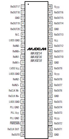
Laser PrintersPinout Specifications
VCC to GND...........................................................-0.5V to +4.0V
VCCO to GND.........................................................-0.5V to +6.0V
RxIN_, RxCLK IN_ to GND ....................................-0.5V to +4.0V
PWRDWN to GND....................................................-0.5V to 6.0V
RxOUT_, RxCLK OUT to GND.....................-0.5V to (VCCO + 0.5V)
Continuous Power Dissipation (TA = +70°C)
48-Pin TSSOP (derate 16mW/°C above +70°C) ..... 1282mW
Storage Temperature Range .........................-65°C to +150°C
Junction Temperature....................................................+150°C
ESD Protection
Human Body Model (RD = 1.5k, CS = 100pF)
All Pins to GND ................................................................±5kV
ISO 10605 (RD = 2k, CS = 330pF)
Contact Discharge (RxIN_, RxCLK IN_) to GND ..............±8kV
Air Discharge (RxIN_, RxCLK IN_) to GND ....................±25kV
Lead Temperature (soldering, 10s) ..............................+300°C
Stresses beyond those listed under "Absolute Maximum Ratings" may cause permanent damage to the device. These are stress ratings only, and functional operation of the device at these or any other conditions beyond those indicated in the operational sections of the specifications is not implied. Exposure to absolute maximum rating conditions for extended periods may affect device reliability.
DescriptionThe MAX9234/MAX9236/MAX9238 deserialize three LVDS serial-data inputs into 21 single-ended LVCMOS/LVTTL outputs. A parallel-rate LVDS clock received with the LVDS data streams provides timing for deserialization. The outputs have a separate supply,allowing 1.8V to 5V output logic levels. All these devices are hot-swappable and allow "on-the-fly" frequency programming.
The MAX9234/MAX9236/MAX9238 feature DC balance,which allows isolation between a serializer and deserializer using AC-coupling. Each deserializer decodes data transmitted by one of the MAX9209/MAX9211/MAX9213/MAX9215 serializers.The MAX9234 has a rising-edge output strobe.
The MAX9236/MAX9238 have a falling-edge output strobe.The MAX9234/MAX9236/MAX9238 operate in DCbalanced mode only.The MAX9234/MAX9236 operate with a parallel input clock of 8MHz to 34MHz, while the MAX9238 operates
from 16MHz to 66MHz. The transition time of the singleended outputs is increased on the low-frequency version parts (MAX9234/MAX9236) for reduced EMI. The LVDS inputs meet ISO 10605 ESD specification, ±25kV for Air Discharge and ±8kV Contact Discharge.
The MAX9234/MAX9236/MAX9238 are available in 48-pin TSSOP packages and operate over the -40°C to +85°C temperature range.

 MAX9234 Data Sheet


