Features: *Programmable DC Balance or Non-DC Balance*DC Balance Allows AC-Coupling for Wider Input Common-Mode Voltage Range*As Low as 8MHz Operation (MAX9210/MAX9212/MAX9220)*Falling-Edge Output Strobe (MAX9220/MAX9222)*Slower Output Transitions for Reduced EMI (MAX9210/MAX9212/MAX9220)*High-Impe...
MAX9220: Features: *Programmable DC Balance or Non-DC Balance*DC Balance Allows AC-Coupling for Wider Input Common-Mode Voltage Range*As Low as 8MHz Operation (MAX9210/MAX9212/MAX9220)*Falling-Edge Output St...
SeekIC Buyer Protection PLUS - newly updated for 2013!
268 Transactions
All payment methods are secure and covered by SeekIC Buyer Protection PLUS.
US $1.34 - 1.34 / Piece
High Speed Operational Amplifiers Op Amp Comparator Reference IC
US $1.6 - 3.31 / Piece
Operational Amplifiers - Op Amps Op Amp Comparator Reference IC
VCC to GND....................................................................-0.5V to +4.0V
VCCO to GND..................................................................-0.5V to +6.0V
RxIN_, RxCLK IN_ to GND...............................................-0.5V to +4.0V
PWRDWN to GND...........................................................-0.5V to +6.0V
DCB/NC to GND.....................................................-0.5V to (VCC+ 0.5V)
RxOUT_, RxCLK OUT to GND..............................-0.5V to (VCCO + 0.5V)
Continuous Power Dissipation (TA= +70°C)
48-Pin TSSOP (derate 16mW/°C above +70°C)................1282mW
48-Lead Thin QFN (derate 26.3mW/°C above +70°C)......2105mW
Storage Temperature Range..................................-65°C to +150°C
Junction Temperature............................................................+150°C
ESD Protection
Human Body Model (RD= 1.5k, CS = 100pF)
All Pins to GND..........................................................................±5kV
IEC 61000-4-2 (RD= 330, CS= 150pF) Level 4
Contact Discharge LVDS Inputs (RxIN_, RxCLK IN_)
to GND......................................................................................±8kA
Air Discharge LVDS Inputs (RxIN_, RxCLK IN_)
to GND....................................................................................±15kV
Lead Temperature (soldering, 10s)..........................................+300
The MAX9210/MAX9212/MAX9214/MAX9216/MAX9220/MAX9222 deserialize three LVDS serial data inputs into 21 single-ended LVCMOS/LVTTL outputs. A parallel rate LVDS clock received with the LVDS data streams provides timing for deserialization. The outputs have a separate supply, allowing 1.8V to 5V output logic levels.
The MAX9210/MAX9212/MAX9214/MAX9216/MAX9220/MAX9222 feature programmable DC balance, which allows isolation between a serializer and deserializer using AC-coupling. Each deserializer decodes data transmitted by one of MAX9209/MAX9211/MAX9213/MAX9215 serializers.
The MAX9210/MAX9212/MAX9214/MAX9216 have rising-edge output strobes, and when DC balance is not programmed, are compatible with non-DC-balanced 21-bit deserializers such as the DS90CR216A and DS90CR218A. The MAX9220/MAX9222 have fallingedge output strobes.
Two frequency versions and two DC-balance default conditions are available for maximum replacement flexibility and compatibility with popular non-DC-balanced deserializers. The transition time of the single-ended outputs is increased on the low-frequency version parts (MAX9210/MAX9212/MAX9220) for reduced EMI. The LVDS inputs meet IEC 61000-4-2 Level 4 ESD specification, ±15kV fo Air Discharge and ±8kV Contact Discharge.
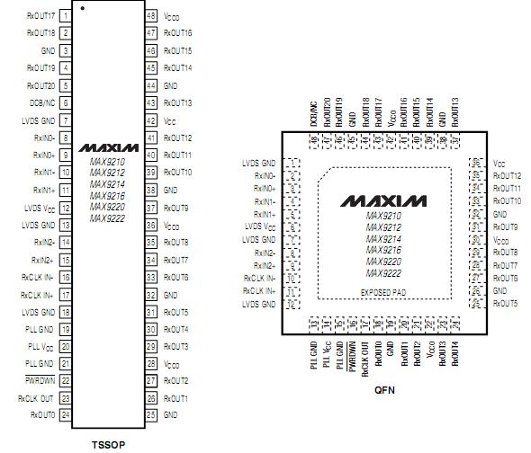
The MAX9210/MAX9212/MAX9214/MAX9216/MAX9220/MAX9222 are available in TSSOP and space-saving QFN packages, and operate over the -40°C to +85°C tempeature range.