Features: ·Proprietary Data Decoding for DC Balance and Reduced EMI
·Control Data Deserialized During Video Blanking
·Five Control Data Inputs Are Single Bit-Error Tolerant
·Output Transition Time Is Scaled to Operating Frequency for Reduced EMI
·Staggered Output Switching Reduces EMI
·Output Enable Allows Busing of Outputs
·Clock Pulse Stretch on Lock
·Wide ±2% Reference Clock Tolerance
·Synchronizes to MAX9217 Serializer Without External Control
·ISO 10605 ESD Protection
·Separate Output Supply Allows Interface to 1.8V to 3.3V Logic
·+3.3V Core Power Supply
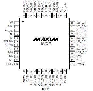
·Space-Saving Thin QFN and TQFP Packages
·-40°C to +85°C Operating TemperatureApplication·Navigation System Display
·In-Vehicle Entertainment System
·Video Camera
·LCD DisplaysPinout Specifications
VCC_ to _GND........................................................-0.5V to +4.0V
Any Ground to Any Ground...................................-0.5V to +0.5V
IN+, IN- to LVDS GND...........................................-0.5V to +4.0V
IN+, IN- Short Circuit to LVDS GND or VCCLVDS ......Continuous
IN+, IN- Short Through 0.125F (or smaller),
25V Series Capacitor..........................................-0.5V to +16V
(R/F, OUTEN, RNG_, REFCLK,
PWRDWN) to GND .................................-0.5V to (VCC + 0.5V)
(RGB_OUT[17:0], CNTL_OUT[8:0], DE_OUT, PCLK_OUT,
LOCK) to VCCO GND...........................-0.5V to (VCCO + 0.5V)
Continuous Power Dissipation (TA = +70°C)
48-Lead TQFP (derate 20.8mW/°C above +70°C) ....1667mW
48-Lead Thin QFN (derate 37mW/°C above +70°C) .2963mW
ESD Protection
Human Body Model (RD = 1.5k, CS = 100pF)
All Pins to GND..............................................................±3.0kV
ISO 10605 (RD = 2k, CS = 330pF)
Contact Discharge (IN+, IN-) to GND ............................±10kV
Air Discharge (IN+, IN-) to GND ....................................±30kV
Storage Temperature Range .........................-65°C to +150°C
Junction Temperature.....................................................+150°C
Lead Temperature (soldering, 10s) ................................+300°C
Stresses beyond those listed under "Absolute Maximum Ratings" may cause permanent damage to the device. These are stress ratings only, and functional operation of the device at these or any other conditions beyond those indicated in the operational sections of the specifications is not implied. Exposure to absolute maximum rating conditions for extended periods may affect device reliability.
DescriptionThe MAX9218 digital video serial-to-parallel converter deserializes a total of 27 bits during data and control phases. In the data phase, the LVDS serial input is converted to 18 bits of parallel video data and in the control phase, the input is converted to 9 bits of parallel control data. The separate video and control phases take advantage of video timing to reduce the serial data rate.The MAX9218 pairs with the MAX9217 serializer to form a complete digital video transmission system.
Proprietary data decoding reduces EMI and provides DC balance. The DC balance allows AC-coupling, providing isolation between the transmitting and receiving ends of the interface. The MAX9218 features a selectable rising or falling output latch edge.
ESD tolerance of MAX9218 is specified for ISO 10605 with ±10kV contact discharge and ±30kV air discharge.
The MAX9218 operates from a +3.3V core supply and features a separate output supply for interfacing to 1.8V to 3.3V logic-level inputs. This device is available in 48-lead Thin QFN and TQFP packages and is specified from -40°C to +85°C.

 MAX9218 Data Sheet


