Features: 1.0ps(RMS)Jitter (max) at 670MHz
68ps(P-P)Jitter at 800Mbps Data Rate
3.3V Supply
LVDS Fail-Safe Inputs (MAX9176)
Anything Inputs (MAX9177) Accept
CML/LVDS/LVPECL
Select and Power-Down Inputs Tolerate -1.0V
and VCC+ 1.0V
Low-Power CMOS Design
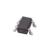
10-Lead µMAX and QFN Packages
-40°C to +85°C Operating Temperature Range
Conform to ANSI TIA/EIA-644 LVDS Standard
IEC61000-4-2 Level 4 ESD Rating ApplicationProtection Switching
Loopback
Clock Distribution
Pinout Specifications
VCC to GND.............................................................-0.3V to +4.0V
IN_+, IN_- to GND..................................................-0.3V to +4.0V
OUT+, OUT- to GND................................................-0.3V to +4.0V
PD, SEL to GND.............................................-1.4V to (VCC+ 1.4V)
Single-Ended and Differential Output
Short-Circuit Duration (OUT+, OUT-)...........................Continuous
Continuous Power Dissipation (TA= +70°C)
10-Pin µMAX (derate 5.6mW/°C above +70°C)................444mW
10-Lead Thin QFN (derate 24.4mW/°C above +70°C)....1951mW
Operating Temperature Range............................-40°C to +85°C
Maximum Junction Temperature.......................................+150°C
Storage Temperature Range.............................-65°C to +150°C
ESD Protection
Human Body Model (RD= 1.5kΩ, CS= 100pF)
(IN_+, IN_-, OUT+, OUT-)...................................................+16kV
IEC61000-4-2 Level 4 (RD= 330Ω, CS= 150pF)
Contact Discharge (IN_+, IN_-, OUT+, OUT-)......................+8 kV
Air-Gap Discharge (IN_+, IN_-, OUT+, OUT-)......................+15kV
Lead Temperature (soldering, 10s)..................................+300°C
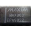
DescriptionThe MAX9176/MAX9177 are 670MHz, low-jitter, low- skew 2:1 multiplexers ideal for protection switching, loopback, and clock distribution. The devices feature ultra-low 68ps peak-to-peak deterministic jitter thatensures reliable operation in high-speed links that are highly sensitive to timing errors.
The MAX9176 has fail-safe LVDS inputs and an LVDS output. The MAX9177 has "anything" differential inputs (CML/LVDS/LVPECL) and an LVDS output. The output can be put into high impedance using the power-down input. The MAX9176 features fail-safe circuits that drive the output high when a selected input is open, undriven and shorted, or undriven and terminated. The MAX9177 has bias circuits that force the output high when a selected input is open. The mux select and power- down inputs are compatible with standard LVTTL/ LVCMOS logic.
The select and power-down inputs tolerate undershoot of -1V and overshoot of VCC + 1V. The MAX9176/MAX9177 are available in 10-pin µMAX and 10-lead thin QFN packages, and operate from a single 3.3V supply over the -40°C to +85°C temperature range.

 MAX9176 Data Sheet


