Features: · Accepts LVDS and LVPECL Inputs
· Fully Compatible with DS90LV048A
· Low 1.0mA (max) Disable Supply Current
· In-Path Fail-Safe Circuitry
· Flow-Through Pinout
Simplifies PC Board Layout
Reduces Crosstalk
· Guaranteed 500Mbps Data Rate
· 400ps Pulse Skew (max)
· Conforms to ANSI TIA/EIA-644 LVDS Standard
· High-Impedance LVDS Inputs when Powered-Off
· Available in Tiny 3mm x 3mm QFN PackageApplication·Digital Copiers
·Laser Printers
·Cellular Phone Base Stations
·Network Switches/Routers
·Backplane Interconnect
·Clock Distribution
·LCD Displays
·Telecom Switching EquipmentPinout Specifications
VCC to GND ..........................................................-0.3V to +4.0V
IN_+, IN_- to GND ...............................................-0.3V to +4.0V
OUT_, EN, EN to GND..................................-0.3V to (VCC + 0.3V)
Continuous Power Dissipation (TA = +70°C)
16-Pin TSSOP (derate 9.4mW/°C above TA = +70°C)..755mW
16-Pin SO (derate 8.7mW/°C above TA = +70°C) .......696mW
16-Pin QFN (derate 14.7mW/°C above TA = +70°C)..1177mW
Junction Temperature....................................................+150°C
Storage Temperature Range ........................-65°C to +150°C
ESD Protection (Human Body Model, IN_+, IN_-) ...........±7.0kV
Lead Temperature (soldering, 10s) ...............................+300°C
Stresses beyond those listed under "Absolute Maximum Ratings" may cause permanent damage to the device. These are stress ratings only, and functional operation of the device at these or any other conditions beyond those indicated in the operational sections of the specifications is not implied. Exposure to absolute maximum rating conditions for extended periods may affect device reliability.
DescriptionThe MAX9173 quad low-voltage differential signaling (LVDS) line receiver is ideal for applications requiring high data rates, low power, and low noise. The MAX9173 is guaranteed to receive data at speeds up to 500Mbps (250MHz) over controlled-impedance media of approximately 100. The transmission media can be printed circuit (PC) board traces or cables.
The MAX9173 accepts four LVDS differential inputs and translates them to LVCMOS/LVTTL outputs. The MAX9173 inputs are high impedance and require an external termination resistor when used in a point-topoint connection.
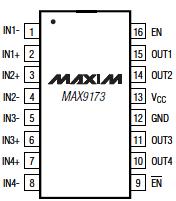
The MAX9173 supports a wide common-mode input range of 0.05V to VCC - 0.05V, allowing for ground potential differences and common-mode noise between the driver and the receiver. A fail-safe feature sets the output high when the inputs are open, or when the inputs are undriven and shorted or undriven and parallel terminated. The EN and EN inputs control the high-impedance outputs. The enables of MAX9173 are common to all four receivers. Inputs conform to the ANSI TIA/EIA-644 LVDS standard. The flow-through pinout simplifies board layout and reduces crosstalk by separating the LVDS inputs and LVCMOS/LVTTL outputs. The MAX9173 operates from a single 3.3V supply, and is specified for operation from -40°C to +85°C. Refer to the MAX9121/ MAX9122 data sheet for lower jitter quad LVDS receivers with parallel fail-safe. Refer to the MAX9123 data sheet for a quad LVDS line driver with flowthrough pinout.
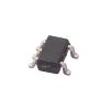
The MAX9173 is available in 16-pin TSSOP, SO, and space-saving thin QFN packages.

 MAX9173 Data Sheet


