Features: BLVDS Signaling
3.3V Operation
Low-Power CMOS Design
200Mbps Data-Signaling Rate
±1V Common-Mode Range
±100mV Receiver Sensitivity
Flow-Through Pinout
Receiver Output High for Undriven Open, Short, or Terminated Input
8-Lead SO PackageApplicationCell-Phone Base Stations
Add/Drop Muxes
Digital Cross-Connects
DSLAMs
Network Switches/Routers
Backplane Interconnect
Clock DistributionPinout Specifications
Vccto GND.........................................................-0.3V to +4.0V
DO+/RI+, DO-/RI- to GND..................................-0.3V to +4.0V
DIN, ROUT, DE, RE to GND .......................-0.3V to (Vcc + 0.3V)
Driver Short-Circuit Current ...................................Continuous
Continuous Power Dissipation (TA = +70°C)
8-Pin SO (derate 5.9mW/°C above +70°C)..................471mW
Operating Temperature Range .......................-40°C to +85°C
Junction Temperature....................................................+150°C
Storage Temperature Range .........................-65°C to +150°C
ESD Protection
HBM (1.5k, 100pF),
DO+/RI+, DO-/RI-, DIN, ROUT, DE, RE..............................> ±2kV
Lead Temperature (soldering, 10s) ................................+300°C
Stresses beyond those listed under "Absolute Maximum Ratings" may cause permanent damage to the device. These are stress ratings only, and functional operation of the device at these or any other conditions beyond those indicated in the operational sections of the specifications is not implied. Exposure to absolute maximum rating conditions for extended periods may affect device reliability.
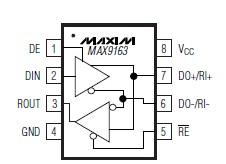
DescriptionThe MAX9163 high-speed bus low-voltage differential signaling (BLVDS) transceiver is designed specifically for heavily loaded multipoint bus applications. The MAX9163 operates from a single 3.3V power supply, and is pin compatible with the DS92LV010A. The transceiver consists of one differential BLVDS line driver and one LVDS receiver. The driver output and receiver input are connected internally to minimize bus loading. The individual enable logic inputs of MAX9163 (DE, RE) are used to enable the driver or the receiver.
The MAX9163 driver output uses a current-steering configuration to generate a 9mA (typ) drive current. The driver accepts a single-ended input and translates it to a differential output level of 243mV (typ) into 27 at speeds up to 200Mbps. The MAX9163 receiver detects a differential input as low as 100mV and translates it to a single-ended output at speeds up to 200Mbps. The receiver input of MAX9163 features a fail-safe circuit that sets the receiver output high when the receiver inputs are undriven and open, terminated, or shorted.
The MAX9163 is offered in an 8-lead SO package, and is specified for operation from -40°C to +85°C.

 MAX9163 Data Sheet


