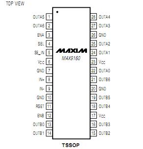
Features: LVDS or LVTTL/LVCMOS Input SelectionLVDS Input Fail-Safe Sets Outputs High for Open,Undriven Short, or Undriven Parallel TerminationTwo Output Banks with Separate Bank EnablesIntegrated Output Series Termination for 60Ω Lines200ps (max) Output-to-Output Skew±100ps (max) Peak-to-Pea...
MAX9160: Features: LVDS or LVTTL/LVCMOS Input SelectionLVDS Input Fail-Safe Sets Outputs High for Open,Undriven Short, or Undriven Parallel TerminationTwo Output Banks with Separate Bank EnablesIntegrated Ou...
SeekIC Buyer Protection PLUS - newly updated for 2013!
268 Transactions
All payment methods are secure and covered by SeekIC Buyer Protection PLUS.
US $1.34 - 1.34 / Piece
High Speed Operational Amplifiers Op Amp Comparator Reference IC
US $1.6 - 3.31 / Piece
Operational Amplifiers - Op Amps Op Amp Comparator Reference IC
The MAX9160 125MHz, 14-port LVTTL/LVCMOS clock driver repeats the selected LVDS or LVTTL/LVCMOS input on two output banks. Each bank consists of seven LVTTL/LVCMOS series terminated outputs and a bank enable. The LVDS input has a fail-safe function. The MAX9160 has a propagation delay that can be adjusted using an external resistor to set the bias current for an internal delay cell. The LVTTL/LVCMOS outputs feature 200ps maximum output-to-output skew and ±100ps maxi-mum added peak-to-peak jitter.The MAX9160 is designed to operate with a 3.3V sup-ply voltage over the extended temperature range of -40°C to +85°C. This MAX9160 is available in 28-pin exposed- and nonexposed-pad TSSOP and 32-lead 5mm x 5mm QFN packages.