Features: Pin Compatible with SN65LVDS9637 Fail-Safe Circuit Sets Output High for Undriven Inputs Conforms to ANSI TIA/EIA-644 Standard Single 3.3V Supply Designed for Data Rates up to 400Mbps ±100mV (max) Differential Input Threshold 2.2ns (typ) Propagation Delay 41mW (typ) Power Dissipation per ...
MAX9159: Features: Pin Compatible with SN65LVDS9637 Fail-Safe Circuit Sets Output High for Undriven Inputs Conforms to ANSI TIA/EIA-644 Standard Single 3.3V Supply Designed for Data Rates up to 400Mbps ±100m...
SeekIC Buyer Protection PLUS - newly updated for 2013!
268 Transactions
All payment methods are secure and covered by SeekIC Buyer Protection PLUS.
US $1.34 - 1.34 / Piece
High Speed Operational Amplifiers Op Amp Comparator Reference IC
US $1.6 - 3.31 / Piece
Operational Amplifiers - Op Amps Op Amp Comparator Reference IC
Vcc to GND..............................................................-0.5V to +4V
1A, 1B, 2A, 2B to GND ............................................-0.5V to +4V
Y1, Y2 to GND ...........................................-0.5V to (VCC + 0.5V)
Continuous Power Dissipation .............................(TA = +70°C)
8-Pin SO (derate 5.88mW/°C above +70°C)................471mW
Maximum Junction Temperature ....................................+150°C
Operating Temperature Range ........................-40°C to +85°C
Storage Temperature Range ..........................-65°C to +150°C
ESD Protection LVDS Inputs (1A, 1B, 2A, 2B)
Human Body Model .............................................................±8kV
Lead Temperature (soldering, 10s) ................................+300°C
Stresses beyond those listed under "Absolute Maximum Ratings" may cause permanent damage to the device. These are stress ratings only, and functional operation of the device at these or any other conditions beyond those indicated in the operational sections of the specifications is not implied. Exposure to absolute maximum rating conditions for extended periods may affect device reliability.
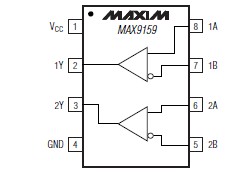
The MAX9159 dual low-voltage differential signaling (LVDS) receiver is ideal for applications requiring high speed, low power, and low noise. The MAX9159 is pin compatible with the SN65LVDS9637. The MAX9159 conforms to the ANSI TIA/EIA-644 LVDS standard and converts LVDS to LVTTL-compatible outputs. A fail-safe feature sets the output high when the inputs are undriven and open, terminated, or shorted. The MAX9159 is available in an 8-pin SO package and fully specified for the -40°C to +85°C extended temperature range.
Refer to the MAX9111/MAX9113 data sheet for higher performance single/dual LVDS line receivers in SOT23 and SO packages. Refer to the MAX9110/MAX9112 data sheet for single/dual LVDS line drivers in SOT23 and SO packages.