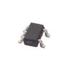
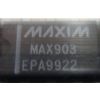
DescriptionThe MAX915 is designed as high speed, single TTL voltage comparator which eliminate oscillation by separating the comparator input and output stages with a negative edgetriggered master/slave flip-flop.MAX915 has ten features. (1)Oscillation free: clocked architecture. (2)6ns propagatio...
MAX915: DescriptionThe MAX915 is designed as high speed, single TTL voltage comparator which eliminate oscillation by separating the comparator input and output stages with a negative edgetriggered master/s...
SeekIC Buyer Protection PLUS - newly updated for 2013!
268 Transactions
All payment methods are secure and covered by SeekIC Buyer Protection PLUS.
US $1.34 - 1.34 / Piece
High Speed Operational Amplifiers Op Amp Comparator Reference IC
US $1.6 - 3.31 / Piece
Operational Amplifiers - Op Amps Op Amp Comparator Reference IC
The MAX915 is designed as high speed, single TTL voltage comparator which eliminate oscillation by separating the comparator input and output stages with a negative edgetriggered master/slave flip-flop.
MAX915 has ten features. (1)Oscillation free: clocked architecture. (2)6ns propagation delay. (3)Propagation delay insensitive to overdrive. (4)Single +5V supplies. (5)2mV input resolution. (6)Input range includes negative supply rall. (7)Low power 14mA (70mW) per conparator, +5V. (8)1.5ns setup time with 5mV overdrive. (9)No minimum requirement for input signal slew rate. (10)Complementary TTL outputs. Those are all the main features.
Some absolute maximum ratings of MAX915 have been concluded into several points as follow. (1)Its positive supply voltage would be +6V. (2)Its negative supply voltage would be -6V. (3)Its differential input voltage would be from (V- -0.3V) to (V+ +0.3V). (4)Its common-mode input voltage would be from (V- -0.3V) to (V+ +0.3V). (5)Its clock input voltage would be from (GND-0.3V) to (V+ +0.3V). (6)Its output short-circuit duration would be continuous to V+, GND and would be 10sec to V-. (7)Its output current would be 20mA. (8)Its continuous power dissipation would be 727mW for 8-pin plastic DIP. (9)Its storage temperature range would be from -65°C to +150°C. (10)Its junction temperature range would be from -65°C to +170°C. (11)Its lead temperature soldering 10sec would be 300°C. It should be noted that stresses above those listed in absolute maximum ratings may cause permanent damage to device.
Also some electrical characteristics of MAX915 are concluded as follow. (1)Its input bias current would be typ 5uA and max 10uA. (2)Its input offset current would be typ 0.2uA and max 1.0uA. (3)Its input referred noise voltage would be typ 600uV and max 900uV. (4)Its input common-mode range would be min V- -0.1V and max V+ -2.2V. (5)Its power-supply rejection ratio would be typ 60uV/V and max 90uV/V. And so on. If you have any question or suggestion or want to know more information about MAX915 please contact us for details. Thank you!