MAX8551: Features: Buck· 100nsQuick-PWM· 95%· 2VApplication·DDR IDDR II·
floor Price/Ceiling Price
- Part Number:
- MAX8551
- Supply Ability:
- 5000
Price Break
- Qty
- 1~5000
- Unit Price
- Negotiable
- Processing time
- 15 Days
SeekIC Buyer Protection PLUS - newly updated for 2013!
- Escrow Protection.
- Guaranteed refunds.
- Secure payments.
- Learn more >>
Month Sales
268 Transactions
Payment Methods
All payment methods are secure and covered by SeekIC Buyer Protection PLUS.
-
Recent History
- What is this?
Description
Features:
Buck
· 100nsQuick-PWM
· 95%
· 2V
Application
·DDR IDDR II
·<
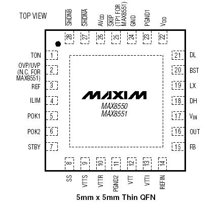
Pinout

Specifications
VIN to GND ............................................................-0.3V to +30V
VDD, AVDD , VTTI to GND .........................................-0.3V to +6V
SHDNA, SHDNB, REFIN to GND.................................-0.3V to +6V
SS, POK1, POK2, SKIP, ILIM, FB to GND ..................-0.3V to +6V
STBY, TON, REF, UVP/OVP to GND ............-0.3V to (AVDD + 0.3V)
OUT, VTTR to GND ....................................-0.3V to (AVDD + 0.3V)
DL to PGND1...............................................-0.3V to (VDD + 0.3V)
DH to LX....................................................-0.3V to (VBST + 0.3V)
LX to BST.................................................................-6V to +0.3V
LX to GND ................................................................-2V to +30V
VTT to GND..............................................-0.3V to (VVTTI + 0.3V)
VTTS to GND............................................-0.3V to (AVDD + 0.3V)
PGND1, PGND2 to GND .......................................-0.3V to +0.3V
REF Short Circuit to GND .........................................Continuous
Continuous Power Dissipation (TA = +70°C)
28-Pin 5mm x 5mm TQFN (derate 35.7mW/°C
above +70°C).................................................................2.86W
Operating Temperature Range ......................-40°C to +85°C
Junction Temperature...................................................+150°C
Storage Temperature Range ........................-65°C to +165°C
Lead Temperature (soldering, 10s) ..............................+300°C
Description
The MAX8550/MAX8551 integrate a synchronous-buck PWM controller to generate VDDQ, a sourcing and sinking LDO linear regulator to generate VTT, and a 10mA reference output buffer to generate VTTR. The buck controller drives two external N-channel MOSFETs to generate output voltages down to 0.7V from a 2V to 28V input with output currents up to 15A. The LDO can sink or source up to 1.5A continuous and 3A peak current. Both the LDO output and the 10mA reference buffer output can be made to track the REFIN voltage. These features make the MAX8550/MAX8551 ideally suited for DDR memory applications in desktops, notebooks, and graphic cards.
The PWM controller in the MAX8550/MAX8551 utilizes Maxim's proprietary Quick-PWM™ architecture with programmable switching frequencies of up to 600kHz. This control scheme handles wide input/output voltage ratios with ease and provides 100ns response to load transients while maintaining high efficiency and a relatively constant switching frequency. The MAX8550 offers fully programmable UVP/OVP and skip-mode options ideal in portable applications. Skip mode allows for improved efficiency at lighter loads. The MAX8551, which is targeted towards desktop and graphic-card applications, does not offer the pulse-skip feature.
The VTT and VTTR outputs of MAX8551 track to within 1% of VREFIN/2. The high bandwidth of this LDO regulator allows excellent transient response without the need for bulk capacitors, thus reducing cost and size.
The buck controller and LDO regulators of MAX8551 are provided with independent current limits. Adjustable lossless foldback current limit for the buck regulator is achieved by monitoring the drain-to-source voltage drop of the low-side MOSFET. Additionally, overvoltage and undervoltage protection mechanisms are built in. Once the overcurrent condition is removed, the regulator is allowed to enter soft-start again. This helps minimize power dissipation during a short-circuit condition. The MAX8550/MAX8551 allow flexible sequencing and standby power management using the active-low SHDNA, active-low SHDNB, and STBY inputs.
Both the MAX8550 and MAX8551 are available in a small 5mm x 5mm, 28-pin thin QFN package.
Customers Who Bought This Item Also Bought
-
US $$1.00 - 2.00 / PieceSupply Ability:10000Week
-
US $$1.00 - 2.00 / PieceSupply Ability:10000Week
-
US $$0.67 - 0.67 / PieceSupply Ability:1000Week
-
US $$2.30 - 2.50 / PieceSupply Ability:8000Day
-
US $$9.40 - 9.78 / PieceSupply Ability:100Week

 MAX8551 Data Sheet


