Features: ♦ MAX8537/MAX8539: Complete DDR Supplies
♦ MAX8538: Dual Nontracking Controller
♦ Out-of-Phase (MAX8537/MAX8538) or In-Phase (MAX8539) Operation
♦ 4.5V to 23V Wide Input Range (Operate Down to 1.8V Input with External 5V Supply)
♦ Tracking Supply Maintains VTT = VTTR = 1/2 VDDQ
♦ Adjustable Output from 0.8V to 3.6V with 1% Accuracy
♦ VTTR Reference Sources and Sinks Up to 15mA
♦ 200kHz to 1.4MHz Adjustable Switching Frequency
♦ All-Ceramic Design Achievable
♦ >90% Efficiency
♦ Independent POK_ and EN_
♦ Adjustable Soft-Start and Soft-Stop for Each Output
♦ Lossless Adjustable-Hiccup Current Limit
♦ Output Overvoltage Protection
♦ 28-Pin QSOP PackageApplicationDDR Memory Power Supplies
Notebooks and Desknotes
Servers and Storage Systems
Broadband Routers
XDSL Modems and Routers
Power DSP Core Supplies
Power Combiner in Advanced VGA Cards
Networking Systems
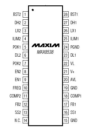
RAMBUS Memory Power SuppliesPinout Specifications
ABSOLUTE MAXIMUM RATINGS
V+ to GND .............................................................-0.3V to +25V
AVL, VL to GND........................................................-0.3V to +6V
PGND to GND .......................................................-0.3V to +0.3V
FB_, EN_, POK_ to GND...........................................-0.3V to +6V
REFIN, VTTR, FREQ, SS_, COMP_ to GND....-0.3V to (AVL + 0.3V)
BST_, ILIM_ to GND ..............................................-0.3V to +30V
DH1 to LX1 ...............................................-0.3V to (BST1 + 0.3V)
DH2 to LX2 ...............................................-0.3V to (BST2 + 0.3V)
LX_ to GND................................................................-2V to +25V
DL_ to PGND ................................................-0.3V to (VL + 0.3V)
Continuous Power Dissipation (TA = +70°C)
28-Pin QSOP (derate 10.8mW/°C above +70°C)........860mW
Operating Temperature Range ........................-40°C to +85°C
Junction Temperature.....................................................+150°C
Storage Temperature Range ..........................-65°C to +150°C
Lead Temperature (soldering, 10s) ............................+300°C
LX_ to BST_ ..............................................................-6V to +0.3V
Stresses beyond those listed under "Absolute Maximum Ratings" may cause permanent damage to the device. These are stress ratings only, and functional operation of the device at these or any other conditions beyond those indicated in the operational sections of the specifications is not implied. Exposure to absolute maximum rating conditions for extended periods may affect device reliability.
DescriptionThe MAX8537/MAX8539 controllers provide a complete power-management solution for both double-data-rate (DDR) and combiner supplies. The MAX8537 and MAX8539 are configured for out-of-phase and in-phase DDR power-supply operations, respectively, and generate three outputs: the main memory oltage (VDDQ), the tracking sinking/sourcing termination voltage (VTT), and the termination reference voltage (VTT). The MAX8538 is configured as a dual out-of-phase controller for pointof- load supplies. Each buck controller can source or sink up to 25A of current, while the termination reference can supply up to 15mA output.
The MAX8537/MAX8538/MAX8539 use constantfrequency voltage-mode architecture with operating frequencies of 200kHz to 1.4MHz. An internal ighbandwidth (25MHz) operational amplifier is used as an error amplifier to regulate the output voltage. This allows fast transient response, reducing the umber of output capacitors. An all-N-FET design optimizes efficiency and cost. The MAX8537/MAX8538/MAX8539 have a 1% accurate reference. The second synchronous buck controller in the MAX8537/MAX8539 and the VTTR amplifier generate 1/2 VDDQ voltage for VTT and VTTR, and track the VDDQ within ± %.
This MAX8538 controllers uses a high-side current-sense architecture for current limiting. ILIM pins allow the setting of an adjustable, lossless current limit for different combinations of load current and RDSON. Alternately, more accurate overcurrent limit is achieved by using a sense resistor in series with the high-side FET. Overvoltage protection of MAX8538 is achieved by latching off the high-side MOSFET and latching on the low-side MOSFET when the output voltage exceeds 7% of its set output. Independent enable, power-good, and soft-start features enhance flexibility.

 MAX8538 Data Sheet


