MAX8500

Features: Integrated Bypass PFET 150mV Dropout at 600mA Load (Regardless of External Inductor) Dynamically Adjustable Output from 0.4V to VBATT Externally Fixed Output from 1.25V to 2.5V with Digitally Controlled High-Power Bypass Mode (MAX8504) 1MHz Fixed-Frequency PWM Switching 600mA Guaranteed...

product image

MAX8500 Picture
SeekIC No. : 004412263 Detail

MAX8500: Features: Integrated Bypass PFET 150mV Dropout at 600mA Load (Regardless of External Inductor) Dynamically Adjustable Output from 0.4V to VBATT Externally Fixed Output from 1.25V to 2.5V with Digit...

floor Price/Ceiling Price

Part Number:
MAX8500
Supply Ability:
5000

Price Break

  • Qty
  • 1~5000
  • Unit Price
  • Negotiable
  • Processing time
  • 15 Days
Total Cost: $ 0.00

SeekIC Buyer Protection PLUS - newly updated for 2013!

  • Escrow Protection.
  • Guaranteed refunds.
  • Secure payments.
  • Learn more >>

Month Sales

268 Transactions

Rating

evaluate  (4.8 stars)

Upload time: 2024/11/27

Payment Methods

All payment methods are secure and covered by SeekIC Buyer Protection PLUS.

Notice: When you place an order, your payment is made to SeekIC and not to your seller. SeekIC only pays the seller after confirming you have received your order. We will also never share your payment details with your seller.
Product Details

Description


Features:

Integrated Bypass PFET
150mV Dropout at 600mA Load (Regardless of External Inductor)
Dynamically Adjustable Output from 0.4V to VBATT
Externally Fixed Output from 1.25V to 2.5V with Digitally Controlled High-Power
    Bypass Mode (MAX8504)
1MHz Fixed-Frequency PWM Switching
600mA Guaranteed Output Current
10% to 100% Duty-Cycle Operation
Low Quiescent Current
    280A (typ) in Normal Mode
    3.3mA (typ) in PWM Mode
    0.1A (typ) in Shutdown Mode
12-Pin Thin QFN (4mm x 4mm, 0.8mm max Height)


Application

N-CDMA/W-CDMA Cellular Phones
Wireless PDAs and Modems


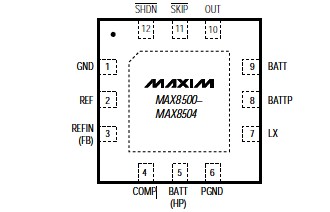
Pinout

  Connection Diagram


Specifications

ABSOLUTE MAXIMUM RATINGS
BATTP, BATT, OUT, SHDN, SKIP, HP,
REFIN, FB to GND ....................................................-0.3V to +6V
PGND to GND .......................................................-0.3V to +0.3V
REF, COMP to GND .................................-0.3V to (VBATT + 0.3V)
LX Current (Note 1) ...........................................................2.25A
Output Short-Circuit Duration .......................................Indefinite
Continuous Power Dissipation (TA = +70°C)
12-Lead Thin QFN (derate 16.9mW/°C above +70°C) .1349mW
Operating Temperature Range .........................-40°C to +85°C
Junction Temperature......................................................+150°C
Storage Temperature Range ...........................-65°C to +150°C
Lead Temperature (soldering, 10s) .................................+300°C

Stresses beyond those listed under "Absolute Maximum Ratings" may cause permanent damage to the device. These are stress ratings only, and functional operation of the device at these or any other conditions beyond those indicated in the operational sections of the specifications is not implied. Exposure to absolute maximum rating conditions for extended periods may affect device reliability.

Note 1: LX has internal clamp diodes to PGND and BATTP. Applications that forward bias these diodes should take care not to exceed the IC's package power dissipation limits.


Description

The MAX8500MAX8504 PWM DC-to-DC buck converters are optimized with integrated bypass FET (0.25 typ) to provide power to the PA in N-CDMA and W-CDMA cell phones. The MAX8500 have a low on-resistance FET to bypass the external inductor for low dropout of only 150mV at 600mA load, regardless of inductor series resistance. The supply voltage range is from 2.6V to 5.5V and the guaranteed converter output current is 600mA. The 1MHz PWM switching frequency of MAX8500 allows for small external components.

The MAX8500MAX8503 are dynamically controlled to provide varying output voltages from 0.4V to VBATT. The LDO regulation point of MAX8500 is slightly lower than the PWM converter such that the transition into and out of dropout is smooth, regardless of the inductor resistance. The MAX8504 is programmed for fixed 1.25V to 2.5V output with external resistors. It features a high-power bypass mode that connects the output directly to the battery. All devices are  esigned to achieve an output settling time of less than 30s for a full-scale change in output voltage and load  urrent.

The MAX8500MAX8504 are available in a 12-lead 4mm x 4mm thin QFN package (0.8mm max height).


Customers Who Bought This Item Also Bought

Margin,quality,low-cost products with low minimum orders. Secure your online payments with SeekIC Buyer Protection.
Test Equipment
Crystals and Oscillators
Semiconductor Modules
Computers, Office - Components, Accessories
Prototyping Products
DE1
Programmers, Development Systems
View more