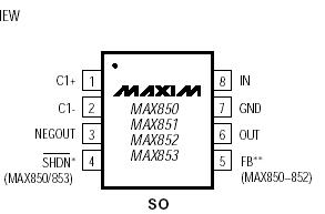
Features: © Fixed -4.1V or Adjustable -0.5V to -9V Output© 4.5V to 10V Input Voltage Range© 2mVp-p Output Voltage Ripple (MAX850MAX852) 1mVp-p Output Voltage Ripple (MAX853)© 100kHz Charge-Pump Switching Frequency (MAX850/MAX851/MAX853)© External Synchronizing Clock Input ...
MAX850: Features: © Fixed -4.1V or Adjustable -0.5V to -9V Output© 4.5V to 10V Input Voltage Range© 2mVp-p Output Voltage Ripple (MAX850MAX852) 1mVp-p Output Voltage Ripple (MAX853)© 100...
SeekIC Buyer Protection PLUS - newly updated for 2013!
268 Transactions
All payment methods are secure and covered by SeekIC Buyer Protection PLUS.
ABSOLUTE MAXIMUM RATINGS
Supply Voltage, VIN to GND ..................................-0.3V to 10.5V
VNEGOUT to GND...................................................-10.5V to 0.3V
VIN to VNEGOUT .......................................................-0.3V to 21V
VOUT to GND (Note 1) .....................................VNEGOUT to 0.3V
SHDN or OSC (pin 4) Voltage to GND............-0.3V to (VIN + 0.3V)
Continuous Power Dissipation (TA = +70°C)
SO (derate 5.88mW/°C above +70°C) .........................471mW
Operating Temperature Ranges
MAX85_ISA........................................................-25°C to +85°C
MAX85_ESA........................................................-40°C to +85°C
Storage Temperature Range ...........................-65°C to +160°C
Lead Temperature (soldering, 10sec) .............................+300°C
Stresses beyond those listed under "Absolute Maximum Ratings" may cause permanent damage to the device. These are stress ratings only, and unctional operation of the device at these or any other conditions beyond those indicated in the operational sections of the specifications is not implied. Exposure to absolute maximum rating conditions for extended periods may affect device reliability.
Note 1: The output may be shorted to NEGOUT or GND if the package power dissipation is not exceeded. Typical short-circuit current to GND is 50mA.
The MAX850MAX853 low-noise, inverting, chargepump power supplies are ideal for biasing GaAsFETs in cellular telephone transmitter amplifiers.
The MAX850MAX852 offer both preset (-4.1V) and adjustable (-0.5V to -9.0V) output voltages. The MAX853 uses an external positive control voltage to set
the negative output voltage. Input voltage range for all four devices is 4.5V to 10V. Output current is 5mA.
An internal linear regulator MAX850 reduces the output voltage ripple to 2mVp-p. With a well-filtered control voltage (VCTRL), the MAX853 achieves typical output ripple of less than 1mVp-p. Supply current is 3mA max, and shutdown current is less than 1µA max over temperature (5µA max for MAX851).