Features: Internal 500mA, 28V N-Channel Switch
(no external FET required)
Adjustable Output Voltage to +27.5V or -27.5V
6-Bit DAC-Controlled Output Voltage
Up to 90% Efficiency
Small 16-Pin QSOP Package
(Same size as 8-pin SO)
Power-OK Indicator
65A Quiescent Current
1.5A Shutdown Current
Up to 300kHz Switching FrequencyApplicationPositive or Negative LCD Bias
Personal Digital Assistants
Notebook Computers
Portable Data-Collection Terminals
Palmtop Computers
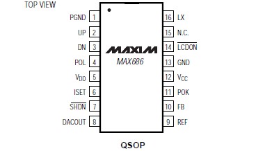
Varactor Tuning Diode BiasPinout Specifications
Voltage
VCC, ISET, POK, POL, SHDN,
UP, DN, VDD to GND...........................................-0.3V to +6V
FB, REF, DACOUT to GND.......................-0.3V to (VCC + 0.3V)
PGND to GND ..................................................-0.3V to +0.3V
LX, LCDON to GND............................................-0.3V to +30V
Current
LX (sinking) ...................................................................600mA
LCDON (sinking)...............................................................10mA
Continuous Power Dissipation (TA = +70°C)
QSOP (derate 8.30mW/°C above +70°C)....................667mW
Operating Temperature Ranges
MAX686C/D ................................................... ......0°C to +70°C
MAX686EEE.......................................................-40°C to +85°C
Storage Temperature Range ..........................-65°C to +160°C
Lead Temperature (soldering, 10sec) ............................+300°C
Stresses beyond those listed under "Absolute Maximum Ratings" may cause permanent damage to the device. These are stress ratings only, and unctional operation of the device at these or any other conditions beyond those indicated in the operational sections of the specifications is not implied. xposure to absolute maximum rating conditions for extended periods may affect device reliability.
DescriptionThe MAX686 DAC-controlled boost/inverter IC converts a positive input voltage to a positive or negative LCD bias voltage up to +27.5V or -27.5V. The MAX686 features an internal N-channel MOSFET switch, programmable current limiting, and an internal 6-bit digital-toanalog converter (DAC) for digital adjustment of the output voltage. It comes in a small 16-pin QSOP package (same size as an 8-pin SO).
The MAX686 uses a current-limited, pulse-frequencymodulation (PFM) control scheme to provide high efficiency over a wide range of load conditions. Its high switching frequency (up to 300kHz) allows the use of small external omponents.
An LCDON output allows the LCD bias voltage to be automatically disabled when the display logic voltage is removed, protecting the display. The MAX686 has a +2.7V to +5.5V input voltage range for the IC, and a +0.8V to +27.5V input voltage range for the inductor. Typical quiescent supply current is 65A. Shutdown current is 1.5A.
The MAX686 offers high-level integration to save space, reduce power consumption, and increase battery life, making it an excellent choice for battery-powered portable equipment. The MAX629 is similar to the MAX686, except that it does not contain a built-in DAC. Both devices have evaluation kits to facilitate designs.

 MAX686 Data Sheet


