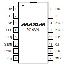
Features: ` Dual Output Using a Single Inductor` Low-Noise Output, 30mVp-p Ripple` Output Voltages up to 24V and down to -9V (up to 45V and down to -16V with added components)` Internal Switches in a Small Package` 220kHz/400kHz Fixed-Frequency PWM Operation` Frequency Can Be Synchronized to Exter...
MAX685: Features: ` Dual Output Using a Single Inductor` Low-Noise Output, 30mVp-p Ripple` Output Voltages up to 24V and down to -9V (up to 45V and down to -16V with added components)` Internal Switches in ...
SeekIC Buyer Protection PLUS - newly updated for 2013!
268 Transactions
All payment methods are secure and covered by SeekIC Buyer Protection PLUS.
US $.38 - .53 / Piece
Voltage & Current References Low-Power Low-Drop Voltage Ref
VDD, VP to GND.......................................................-0.3V to +6V
PGND to GND .......................................................-0.3V to +0.3V
VDD to VP.............................................................-0.3V to +0.3V
LXN, POK to GND ..................................................-0.3V to +30V
LXP to VDD.............................................................-15V to +0.3V
REF, SEQ, SHDN to GND..............................-0.3V to (VDD + 0.3V)
FBP, FBN, SYNC to GND ...........................................-0.3V to +6V
Continuous Power Dissipation (TA = +70°C)
16-Pin QSOP (derate 8.3mW/°C above +70°C)............667mW
Operating Temperature Range ........................-40°C to +85°C
Junction Temperature.....................................................+150°C
Storage Temperature Range ..........................-65°C to +165°C
Lead Temperature (soldering, 10sec) ............................+300°C
Stresses beyond those listed under "Absolute Maximum Ratings" may cause permanent damage to the device. These are stress ratings only, and functional operation of the device at these or any other conditions beyond those indicated in the operational sections of the specifications is not implied. Exposure to absolute maximum rating conditions for extended periods may affect device reliability.
The MAX685 DC-DC converter provides low-noise dual outputs for powering CCD imaging devices and LCDs. This device uses a single inductor to provide independently regulated positive and negative outputs. Integrated power switches are included in the small 16-pin QSOP package (same size as an 8-pin SO) to save space and reduce cost.
Each output of MAX685 delivers up to 10mA from a +2.7V to +5.5V input voltage range. Output voltages are set independently up to 24V and down to -9V. With a few additional low-cost components, the output voltages can be set at up to 45V and down to -16V. Output ripple magnitude is 30mVp-p. The MAX685 uses a fixed-frequency, pulsewidth- modulated (PWM) control scheme at 220kHz or 400kHz to permit output noise filtering and to reduce the size of external components. The frequency can also be synchronized to an external clock signal between 200kHz and 480kHz.
The MAX685 has a power-OK indicator output (POK) that signals when both outputs are within regulation. A logic-controlled shutdown completely turns off both outputs and reduces supply current to 0.1A. The user can also set which output turns on first.
The preassembled MAX685 evaluation kit is available to reduce design time.