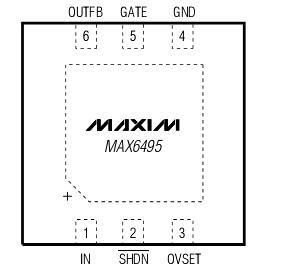
Features: Wide Supply Voltage Range: +5.5V to +72V
Overvoltage-Protection Switch Controller Allows
User to Size External n-Channel MOSFETs
Fast Gate Shutoff During Overvoltage with 100mA
Sink Capability
Internal Charge-Pump Circuit Ensures 10V
Gate-to-Source Enhancement for Low RDS(ON)
Performance
n-Channel MOSFET Latches Off After an
Overvoltage Condition (MAX6497/MAX6499)
Adjustable Overvoltage Threshold
Thermal Shutdown Protection
Supports Series p-Channel MOSFET for Reverse-
Battery Voltage Protection (MAX6496)
POK Indicator (MAX6497/MAX6498)
Adjustable Undervoltage Threshold (MAX6499)
-40°C to +125°C Operating Temperature Range
Small, 3mm x 3mm TDFN PackageApplicationAutomotive
Industrial
Telecom/Servers/Networking
FireWire(R)
Notebook ComputersPinout Specifications
IN, GATE, GATEP......................................................-0.3V to +80V
SHDN, CLEAR................................................-0.3V to (VIN + 0.3V)
POK, OUTFB.............................................................-0.3V to +80V
GATE to OUTFB........................................................-0.3V to +12V
GATEP to IN.............................................................-12V to +0.3V
OVSET, UVSET, POKSET...........................................-0.3V to +12V
Current Sink/Source (All Pins)...............................................50mA
All Other Pins to GND.....................................-0.3V to (VIN + 0.3V)
Continuous Power Dissipation (TA = +70°C)
6-Pin TDFN (derate 18.2mW/°C above +70°C) ............1455mW
8-Pin TDFN (derate 18.2mW/°C above +70°C) ............1455mW
Operating Temperature Range .......................-40°C to +125°C
Junction Temperature......................................................+150°C
Storage Temperature Range...........................-60°C to +150°C
Lead Temperature (soldering, 10s).................................+300°C
DescriptionThe MAX6496 is a family of small, low-cur- rent, overvoltage-protection circuits for high-voltagetransient systems such as those found in automotive and industrial applications. These devices monitor the input voltage and control an external n-channel MOSFET switch to isolate the load at the output during an input overvoltage condition. The MAX6496 operateover a wide supply voltage range from +5.5V to +72V.
The gate of the n-channel MOSFET MAX6496 is driven high while the monitored input is below the user-adjustable over- voltage threshold. An integrated charge-pump circuit provides a 10V gate-tosource voltage to fully enhance the n-channel MOSFET. When the input voltage exceeds the user-adjusted overvoltage threshold, the gate of the MOSFET MAX6496 is quickly pulled low, disconnect-ing the load from the input. In some applications, dis- connecting the output from the load is not desirable. In these cases, the protection circuit can be configured toact as a voltage limiter where the GATE output saw-tooths to limit the voltage to the load (MAX6495/MAX6496/MAX6499).
The MAX6496 supports lower input voltages and reduces power loss by replacing the external reverse battery diode with an external series p-channel MOSFET.
The MAX6496 generates the proper bias voltage to ensure that the p-channel MOSFET is on during normal operations. The gate-to-source voltage is clamped dur-ing load-dump conditions, and the p-channel MOSFET is off during reverse-battery conditions. The MAX6497/MAX6498 feature an open-drain, undedi-cated comparator that notifies the system if the output falls below the programmed threshold. The MAX6497 keeps the MOSFET switch latched off until either the input power or the SHDN pin is cycled. The MAX6498 will autoretry when VOVSET falls below 130mV.These devices are available in small, thermally enhanced, 6-pin and 8-pin TDFN packages and are fully specified from -40°C to +125°C.

 MAX6496 Data Sheet


