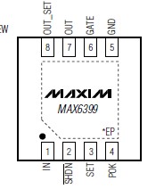
Features: ·Wide Supply Voltage Range (5.75V to 72V)·Internal Charge Pump Ensures n-Channel MOSFET is Fully Enhanced During Normal Operation (VGS = 10V) ·Fast GATE Shutoff During Overvoltage with 20mA Sink Capability·Latches Off External n-Channel MOSFET During High-Voltage Transients·Adjustable DC...
MAX6399: Features: ·Wide Supply Voltage Range (5.75V to 72V)·Internal Charge Pump Ensures n-Channel MOSFET is Fully Enhanced During Normal Operation (VGS = 10V) ·Fast GATE Shutoff During Overvoltage with 20m...
SeekIC Buyer Protection PLUS - newly updated for 2013!
268 Transactions
All payment methods are secure and covered by SeekIC Buyer Protection PLUS.
US $.38 - .53 / Piece
Voltage & Current References Low-Power Low-Drop Voltage Ref
IN, GATE, OUT .......................................................-0.3V to +80V
SHDN............................................................-0.3V to (IN + 0.3V)
OUT .......................................................................-0.3V to +80V
GATE to OUT..........................................................-0.3V to +20V
OUT_SET, SET, POK ..............................................-0.3V to +12V
Maximum Current (All pins) ................................................50mA
Continuous Power Dissipation (TA = +70°C)
8-Pin TDFN (derate 18.2mW/°C above +70°C) .........1455mW
Operating Temperature Range .....................-40°C to +125°C
Junction Temperature....................................................+150°C
Storage Temperature Range .........................-65°C to +150°C
Lead Temperature Range...............................................+300°C
Stresses beyond those listed under "Absolute Maximum Ratings" may cause permanent damage to the device. These are stress ratings only, and functional operation of the device at these or any other conditions beyond those indicated in the operational sections of the specifications is not implied. Exposure to absolute maximum rating conditions for extended periods may affect device reliability.
The MAX6399 is a small overvoltage and undervoltage protection circuit. The device can monitor a DC-DC output voltage and quickly disconnect the power source from the DC-DC input load when an overvoltage condition occurs. A power-OK output signals when the DC-DC input voltage falls below an adjustable threshold. This controller architecture provides the ability to size the external n-channel MOSFET to meet specific load current requirements.
When the DC-DC monitored output voltage is below the user-adjustable overvoltage threshold, the GATE output of the MAX6399 goes high to enhance the n-channel MOSFET. The MAX6399 offers internal charge-pump circuitry that allows the GATE voltage to be 10V above the input voltage (VGS = 10V) to fully enhance the exter nal n-channel MOSFET, thus minimizing the drainto- source resistance.
When the monitored output voltage of MAX6399 rises above the user-adjusted overvoltage threshold, the GATE output rapidly pulls low to shut off the MOSFET. The MOSFET remains latched off until either the MAX6399 input power or SHDN input is cycled. The MAX6399 includes a logic-low shutdown input that disables the GATE. An internal overtemperature detector also disables the gate when the MAX6399 temperature reaches the thermal- shutdown threshold.
The device operates over a wide supply voltage range (5.75V to 72V) and is offered in a small TDFN package, fully specified from -40°C to +125°C.