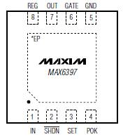
Features: ` 5.5V to 72V Wide Supply Voltage Range
` Overvoltage Protection Controllers Allow User to Size External n-Channel MOSFETs
` Internal Charge-Pump Circuit Ensures MOSFET Gate-to-Source Enhancement for Low RDS(ON) Performance
` Disconnect or Limit Output from Input During Overvoltage Conditions
` Adjustable Overvoltage Threshold
` Thermal-Shutdown Protection
` Always-On, Low-Current (37A) Linear Regulator Sources Up to 100mA (MAX6397)
` Fully Specified from -40°C to +125°C (TJ)
` Small, Thermally Enhanced 3mm x 3mm TDFN PackageApplication·Automotive
·Industrial
·FireWire®
·Notebook Computers
·Wall Cube Power DevicesPinout Specifications
(All pins referenced to GND, unless otherwise noted.)
IN, GATE, OUT ......................................................-0.3V to +80V
SHDN............................................................-0.3V to (IN + 0.3V)
GATE to OUT ..........................................................-0.3 to +20V
SET, REG, POK .....................................................-0.3V to +12V
Maximum Current:
IN, REG...........................................................................350mA
All Remaining Pins ............................................................50mA
Continuous Power Dissipation (TA = +70°C)
6-Pin TDFN (derate 18.2mW/°C above +70°C) ........1455mW
8-Pin TDFN (derate 18.2mW/°C above +70°C) .........1455mW
Operating Temperature Range (TA) .............-40°C to +125°C
Junction Temperature...................................................+150°C
Storage Temperature Range ........................-65°C to +150°C
Lead Temperature .......................................................+300°C
Stresses beyond those listed under "Absolute Maximum Ratings" may cause permanent damage to the device. These are stress ratings only, and functional operation of the device at these or any other conditions beyond those indicated in the operational sections of the specifications is not implied. Exposure to absolute maximum rating conditions for extended periods may affect device reliability.
DescriptionThe MAX6397/MAX6398 are small, high-voltage overvoltage protection circuits. These devices disconnect the output load or limit the output voltage during an input overvoltage condition. These devices are ideal for applications that must survive high-voltage transients such as those found in automotive and industrial applications.
The MAX6397/MAX6398 monitor the input or output voltages and control an external n-channel MOSFET to isolate or limit the load from overvoltage transient energy.When the monitored input voltage is below the useradjustable overvoltage threshold, the external n-channel MOSFET is turned on by the GATE output. In this mode,the internal charge pump fully enhances the n-channel MOSFET with a 10V gate-to-source voltage.
When the input voltage of MAX6397 exceeds the overvoltage threshold,the protection can disconnect the load from the input by quickly forcing the GATE output low. In some applications, disconnecting the output from the load is not desirable. In these cases, the protection circuit can be configured to act as a voltage limiter where the GATE output sawtooths to limit the voltage to the load.
The MAX6397 also offers an always-on linear regulator that is capable of delivering up to 100mA of output current. This high-voltage linear regulator consumes only 37A of quiescent current.The regulator is offered with output options of 5V, 3.3V, 2.5V, or 1.8V. An open-drain, power-good output (POK) asserts when the regulator output falls below 92.5% or 87.5% of its nominal voltage.
The MAX6397/MAX6398 include internal thermal-shutdown protection, disabling the external MOSFET and linear regulator if the chip reaches overtemperature conditions. The devices operate over a wide 5.5V to 72V supply voltage range, are available in small TDFN packages, and are fully specified from -40°C to +125°C.

 MAX6397 Data Sheet


