Features: ·200Msps Output Update Rate
·Single 3.3V Supply Operation
·Excellent SFDR and IMD Performance
SFDR = 77dBc at fOUT = 10MHz (to Nyquist)
IMD = -88dBc at fOUT = 10MHz
ACLR = 74dB at fOUT = 30.72MHz
·2mA to 20mA Full-Scale Output Current
·CMOS-Compatible Digital and Clock Inputs
·On-Chip 1.2V Bandgap Reference
·Low Power Dissipation
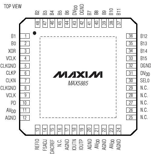
·48-Pin QFN-EP PackageApplication·Base Stations: Single/Multicarrier UMTS,
·CDMA, GSM
·Communications: LMDS, MMDS, Point-to-Point
·Microwave
·Digital Signal Synthesis
·Automated Test Equipment (ATE)
·InstrumentationPinout Specifications
AVDD, DVDD, VCLK to AGND............................................-0.3V to +3.9V
AVDD, DVDD, VCLK to DGND ...........................................-0.3V to +3.9V
AVDD, DVDD, VCLK to CLKGND .......................................-0.3V to +3.9V
AGND, CLKGND to DGND................................................-0.3V to +0.3V
DACREF, REFIO, FSADJ to AGND........................ ..-0.3V to AVDD + 0.3V
IOUTP, IOUTN to AGND...........................................-1V to AVDD + 0.3V
CLKP, CLKN to CLKGND.......................................-0.3V to VCLK + 0.3V
B0B15, SEL0, PD, XOR to DGND.......................-0.3V to DVDD + 0.3V
Continuous Power Dissipation (TA = +70°C)
48-Pin QFN (derate 27mW/°C above +70°C)...................2162.2mW
Thermal Resistance (JA) ....................................................+37°C/W
Operating Temperature Range ................................-40°C to +85°C
Junction Temperature.............................................................+150°C
Storage Temperature Range .................................-60°C to +150°C
Lead Temperature (soldering, 10s) .......................................+300°C
Stresses beyond those listed under "Absolute Maximum Ratings" may cause permanent damage to the device. These are stress ratings only, and functional operation of the device at these or any other conditions beyond those indicated in the operational sections of the specifications is not implied. Exposure to absolute maximum rating conditions for extended periods may affect device reliability.
DescriptionThe MAX5885 is an advanced, 16-bit, 200Msps digitalto-analog converter (DAC) designed to meet the demanding performance requirements of signal synthesis applications found in wireless base stations and other communications applications. Operating from a single 3.3V supply, this DAC offers exceptional dynamic performance such as 77dBc spurious-free dynamic range (SFDR) at fOUT = 10MHz. The DAC supports update rates of 200Msps at a power dissipation of less than 200mW.
The MAX5885 utilizes a current-steering architecture, which supports a full-scale output current range of 2mA to 20mA, and allows a differential output voltage swing between 0.1VP-P and 1VP-P.
The MAX5885 features an integrated 1.2V bandgap reference and control amplifier to ensure high accuracy and low noise performance. Additionally, a separate reference input pin enables the user to apply an external reference source for optimum flexibility and to improve gain accuracy.
The digital and clock inputs of the MAX5885 are designed for CMOS-compatible voltage levels. The MAX5885 is available in a 48-pin QFN package with an exposed paddle (EP) and is specified for the extended industrial temperature range (-40°C to +85°C).
Refer to the MAX5883 and MAX5884 data sheets for pin-compatible 12- and 14-bit versions of the MAX5885. For LVDS high-speed versions, refer to the MAX5886/MAX5887/MAX5888 data sheet.

 MAX5885 Data Sheet


