MAX5754

Features: · Guaranteed Monotonic to 14 Bits· 32 Individual DACs in an 8mm x 8mm, 56-Pin, Thin QFN Package· Three Output Voltage Ranges 0 to +10V (MAX5753)-2.5V to +7.5V (MAX5754)-5V to +5V (MAX5755)· Buffered Voltage Outputs Capable of Driving 10kΩ || 100pF· Glitch-Free Power-Up· SPI-/QSPI-/...

product image

MAX5754 Picture
SeekIC No. : 004411365 Detail

MAX5754: Features: · Guaranteed Monotonic to 14 Bits· 32 Individual DACs in an 8mm x 8mm, 56-Pin, Thin QFN Package· Three Output Voltage Ranges 0 to +10V (MAX5753)-2.5V to +7.5V (MAX5754)-5V to +5V (MAX5755)...

floor Price/Ceiling Price

Part Number:
MAX5754
Supply Ability:
5000

Price Break

  • Qty
  • 1~5000
  • Unit Price
  • Negotiable
  • Processing time
  • 15 Days
Total Cost: $ 0.00

SeekIC Buyer Protection PLUS - newly updated for 2013!

  • Escrow Protection.
  • Guaranteed refunds.
  • Secure payments.
  • Learn more >>

Month Sales

268 Transactions

Rating

evaluate  (4.8 stars)

Upload time: 2024/11/27

Payment Methods

All payment methods are secure and covered by SeekIC Buyer Protection PLUS.

Notice: When you place an order, your payment is made to SeekIC and not to your seller. SeekIC only pays the seller after confirming you have received your order. We will also never share your payment details with your seller.
Product Details

Description


Features:

· Guaranteed Monotonic to 14 Bits
· 32 Individual DACs in an 8mm x 8mm, 56-Pin, Thin QFN Package
· Three Output Voltage Ranges
0 to +10V (MAX5753)
-2.5V to +7.5V (MAX5754)
-5V to +5V (MAX5755)
· Buffered Voltage Outputs Capable of Driving 10kΩ || 100pF
· Glitch-Free Power-Up
· SPI-/QSPI-/MICROWIRE-/DSP-Compatible 33MHz Serial Interface


Application

·Automatic Test Systems
·Optical Router Controls
·Industrial Process Controls
·Arbitrary Function Generators
·Avionics Equipment
·Digital Offset/Gain Adjustment


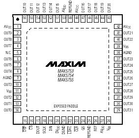
Pinout

  Connection Diagram


Specifications

AVCC to VSS, AGND, DGND, REFGND.......................-0.3V to +12V
VSS to AGND, DGND..................................................-6V to +0.3V
AVDD, DVDD to AGND, DGND, REFGND.......................-0.3V to +6V
AGND to DGND.......................................................-0.3V to +0.3V
REF to AGND, DGND,
REFGND..................-0.3V to the lower of (AVDD + 0.3V) and +6V
REFGND to AGND...................................................-0.3V to +0.3V
Digital Inputs to AGND, DGND,
REFGND..................-0.3V to the lower of (DVDD + 0.3V) and +6V
DOUT to DGND.......-0.3V to the lower of (DVDD + 0.3V) and +6V
OUT_ to VSS.........-0.3V to the lower of (AVCC + 0.3V) and +12V
GS to AGND ................................................................-1V to +1V
Maximum Current into REF...............................................±10mA
Maximum Current into Any Pin ........................................±50mA
Continuous Power Dissipation (TA = +70°C)
Thin QFN (derate 31.3mW/°C above +70°C)....................2.5W
Thin QFP (derate 25mW/°C above +70°C) .......................2.0W
Operating Temperature Range............................0°C to +85°C
Junction Temperature....................................................+150°C
Storage Temperature Range .............................-65°C to +150°C
Lead Temperature (soldering, 10s) .................................+300°C


Description

The MAX5753/MAX5754/MAX5755 are 32-channel, 14- bit, voltage-output, digital-to-analog converters (DACs). All devices accept a 3V external reference input. The devices include an internal offset DAC that allows all the outputs to be offset and a ground-sensing function, allowing output voltages to be referenced to a remote ground. A 33MHz SPI™-/QSPI™-/MICROWIRE™- and digital signal processor (DSP)-compatible serial interface controls the MAX5753/MAX5754/MAX5755. Each DAC has a double-buffered input structure that helps minimize the digital noise feedthrough from the digital inputs to the outputs, and allows for synchronous or asynchronous updating of the outputs. The MAX5753/MAX5754/MAX5755 also provide a DOUT that allows for read-back or daisy chaining multiple devices. The devices provide separate power inputs for the analog and digital sections and provide separate power inputs for the output buffer amplifiers. The MAX5753/MAX5754/MAX5755 include proprietary deglitch circuits to prevent output glitches at power-up and eliminate the need for power sequencing. The devices provide a software-shutdown mode to allow efficient power management. The MAX5753/MAX5754/MAX5755 consume 50µA of supply current in shutdown.

The MAX5753/MAX5754/MAX5755 provide buffered outputs that can drive 10kΩ in parallel with 100pF. The MAX5753 has a 0 to +10V range; the MAX5754 has a -2.5V to +7.5V range; the MAX5755 has a -5V to +5V range. The MAX5753/MAX5754/MAX5755 are available in 56-pin, 8mm x 8mm, thin QFN or 64-pin thin QFP packages and operate over the 0°C to +85°C temperature range.


Customers Who Bought This Item Also Bought

Margin,quality,low-cost products with low minimum orders. Secure your online payments with SeekIC Buyer Protection.
Connectors, Interconnects
Crystals and Oscillators
Semiconductor Modules
Soldering, Desoldering, Rework Products
Line Protection, Backups
View more