Features: Operate from Single +5V Supply
Buffered Voltage Output
Internal 2.048V Reference (MAX531)
140µA Supply Current (MAX538/MAX539)
INL = ±1/2LSB (max)
Guaranteed Monotonic over Temperature
Flexible Output Ranges:
0V to VDD (MAX531/MAX539)
VSS to VDD (MAX531)
0V to 2.6V (MAX531/MAX538)
8-Pin SO/DIP (MAX538/MAX539)
Power-On Reset
Serial Data Output for Daisy-ChainingApplicationBattery-Powered Test Instruments
Digital Offset and Gain Adjustment
Battery-Operated/Remote Industrial Controls
Machine and Motion Control Devices
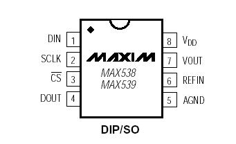
Cellular TelephonesPinout Specifications
VDD to DGND and VDD to AGND ...................................-0.3V, +6V
VSS to DGND and VSS to AGND ....................................-6V, +0.3V
VDD to VSS.................................................................-0.3V, +12V
AGND to DGND...........................................................-0.3V, +0.3V
Digital Input Voltage to DGND .......................-0.3V, (VDD + 0.3V)
REFIN ..................................................(VSS - 0.3V), (VDD + 0.3V)
REFOUT to AGND ...........................................-0.3V, (VDD + 0.3V)
RFB .....................................................(VSS - 0.3V), (VDD + 0.3V)
BIPOFF................................................(VSS - 0.3V), (VDD + 0.3V)
VOUT (Note 1) ..............................................................VSS, VDD
Continuous Current, Any Pin...............................-20mA, +20mA
Continuous Power Dissipation (TA = +70°C)
8-Pin Plastic DIP (derate 9.09mW/°C above +70°C).....727mW
8-Pin SO (derate 5.88mW/°C above +70°C) ................471mW
14-Pin Plastic DIP (derate 10.00mW/°C above +70°C..800mW
14-Pin SO (derate 8.33mW/°C above +70°C) ..............667mW
Operating Temperature Ranges
MAX53_ _C_ _ .....................................................0°C to +70°C
MAX53_ _E_ _ ..................................................-40°C to +85°C
Storage Temperature Range ..........................-65°C to +165°C
Lead Temperature (soldering, 10sec) .............................+300°C
Note 1: The output may be shorted to VDD, VSS, or AGND if the package power dissipation limit is not exceeded.
Stresses beyond those listed under "Absolute Maximum Ratings" may cause permanent damage to the device. These are stress ratings only, and functional operation of the device at these or any other conditions beyond those indicated in the operational sections of the specifications is not implied. Exposure to absolute maximum rating conditions for extended periods may affect device reliability.
DescriptionThe MAX531/MAX538/MAX539 are low-power, voltageoutput, 12-bit digital-to-analog converters (DACs) specified for single +5V power-supply operation. The MAX531 can also be operated with ±5V supplies. The MAX538/MAX539 draw only 140µA, and the MAX531 (with internal reference) draws only 260µA. The
MAX538/MAX539 come in 8-pin DIP and SO packages, while the MAX531 comes in 14-pin DIP and SO packages. All parts have been trimmed for offset voltage, gain, and linearity, so no further adjustment is necessary.
The MAX538's buffer is fixed at a gain of +1 and the MAX539's buffer at a gain of +2. The MAX531's internal op amp may be configured for a gain of +1 or +2, as well as for unipolar or bipolar output voltages. The MAX531 can also be used as a four-quadrant multiplier without external resistors or op amps.
For parallel data inputs, see the MAX530 data sheet.

 MAX539 Data Sheet


