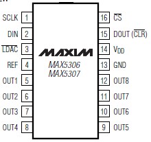
Features: ` Eight Highly Integrated 12-Bit DACs in 16-Pin TSSOP (6.4mm x 5mm) Package` Ultra-Low Glitch Energy <2nV/s` Low Total Supply Current: 1.7mA (max) with VREF = VDD = +5.5V` +2.7V to +5.5V Wide Single-Supply Range` Fast 5s Settling Time` Software-Selectable Shutdown Mode < 1A` 15MHz ...
MAX5307: Features: ` Eight Highly Integrated 12-Bit DACs in 16-Pin TSSOP (6.4mm x 5mm) Package` Ultra-Low Glitch Energy <2nV/s` Low Total Supply Current: 1.7mA (max) with VREF = VDD = +5.5V` +2.7V to +5.5...
SeekIC Buyer Protection PLUS - newly updated for 2013!
268 Transactions
All payment methods are secure and covered by SeekIC Buyer Protection PLUS.
Features: ·+5V at 10A Output·±36V to ±72V Input Voltage Range·250kHz Switching Frequency·Fully Iso...
VDD to GND............................................................. -0.3V to +6V
All Other Pins to GND.................................-0.3V to (VDD + 0.3V)
Continuous Power Dissipation (TA = +70°C)
16-Pin TSSOP (derate 9.4mW/°C above +70°C) .........775mW
Maximum Current Into Any Pin .......................................±50mA
Operating Temperature Range .......................-40°C to +85°C
Junction Temperature....................................................+150°C
Storage Temperature Range .........................-65°C to +150°C
Lead Temperature (soldering, 10s) ...............................+300°C
Stresses beyond those listed under "Absolute Maximum Ratings" may cause permanent damage to the device. These are stress ratings only, and functional operation of the device at these or any other conditions beyond those indicated in the operational sections of the specifications is not implied. Exposure to absolute maximum rating conditions for extended periods may affect device reliability.
The MAX5306/MAX5307 are 12-bit, eight channel, lowpower, voltage-output, digital-to-analog converters (DACs) in a space-saving 16-pin TSSOP package. The wide +2.7V to +5.5V supply voltage range and less than 215A (max) supply current per DAC are excellent for low-power and low-voltage applications. The low 2nV/s glitch energy of the MAX5306/MAX5307 makes them ideal for digital control of fast-response, closedloop systems.
The MAX5306 has a digital output (DOUT) that can be used for daisy-chaining multiple devices. The MAX5307 has a hardware reset input (CLR) which clears all registers and DACs to zero. The MAX5306/MAX5307 have a software shutdown feature that reduces the supply current to 1A. The MAX5306/MAX5307 feature a load DAC (LDAC) function that updates the output of all eight DACs simultaneously.
The 3-wire SPI™, QSPI™, MICROWIRE™ and DSPcompatible serial interface allows the input and DAC registers to be updated independently or simultaneously with a single software command. These devices use a double-buffered design to minimize the digital-noise feedthrough from the digital inputs to the outputs.
The MAX5306/MAX5307 operating temperature range is from -40°C to +85°C.