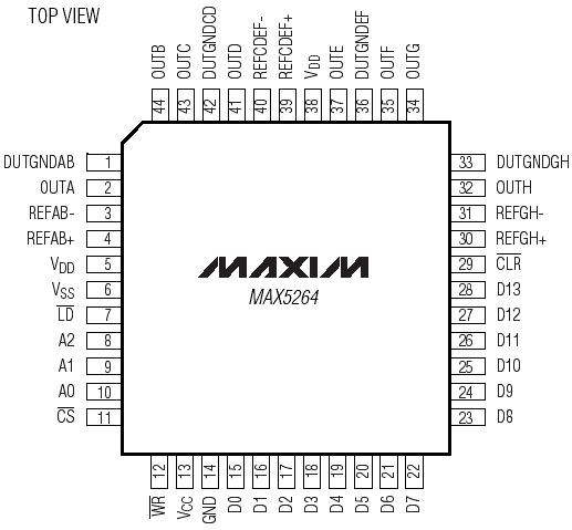
Features: · Full 14-Bit Performance Without Adjustments
· 8 DACs in a Single Package
· Buffered Voltage Outputs
· Unipolar or Bipolar Voltage Swing to +9V and -4V
· 22µs Output Settling Time
· Drives Up to 10,000pF Capacitive Load
· Low Output Glitch: 30mV
· Low Power Consumption: 10mA (typ)
· Small 44-Pin MQFP Package
· Double-Buffered Digital Inputs
· Asynchronous Load Updates All DACs Simultaneously
· Asynchronous CLR Forces All DACs to DUTGND PotentialApplication·Automatic Test Equipment (ATE)
·Industrial Process Controls
·Arbitrary Function Generators
·Avionics Equipment
·Minimum Component Count Analog Systems
·Digital Offset/Gain Adjustment
·SONET ApplicationsPinout Specifications
VDD to GND ..............................................................-0.3V to +16.8V
VSS to GND ...............................................................-10.8V to +0.3V
VCC to GND ...................................................................-0.3V to +6V
A_, D_, WR, CS, LD, CLR to GND......................+0.3V to (VCC + 0.3V)
REF_ _ _ _+, REF_ _ _ _-,
DUTGND_ _ ...........................................(VSS - 0.3V) to (VDD + 0.3V)
OUT_ ...............................................................................VDD to VSS
Maximum Current into REF_ _ _ _ _, DUTGND_ _ .................±10mA
Maximum Current into Any Signal Pin ...................................±50mA
OUT_ Short-Circuit Duration to VDD, VSS, and GND ......................1s
Continuous Power Dissipation (TA = +70°C)
44-Pin MQFP (derate 11.1mW/°C above +70°C)................870mW
Operating Temperature Range.................................0°C to +70°C
Junction Temperature..........................................................+150°C
Storage Temperature Range ...............................-65°C to +150°C
Lead Temperature (soldering, 10s) .....................................+300°C
Stresses beyond those listed under "Absolute Maximum Ratings" may cause permanent damage to the device. These are stress ratings only, and functional operation of the device at these or any other conditions beyond those indicated in the operational sections of the specifications is not implied. Exposure to absolute maximum rating conditions for extended periods may affect device reliability.
DescriptionThe MAX5264 contains eight 14-bit, voltage-output digital-to-analog converters (DACs). On-chip precision output amplifiers provide the voltage outputs. The device operates from +14V/-9V supplies. Its bipolar output voltage swing ranges from +9V to -4V and is achieved with no external components. The MAX5264 has three pairs of differential reference inputs; two of these pairs are connected to two DACs each, and a third pair is connected to four DACs. The references are independently controlled, providing different full-scale output voltages to the respective DACs. The MAX5264 operates within the following voltage ranges: VDD = +7V to +14V, VSS = -5V to -9V, and VCC = +4.75V to +5.25V.
The MAX5264 features double-buffered interface logic with a 14-bit parallel data bus. Each DAC has an input latch and a DAC latch. Data in the DAC latch sets the output voltage. The eight input latches are addressed with three address lines. Data is loaded to the input latch with a single write instruction. An asynchronous load input (LD) transfers data from the input latch to the DAC latch. The LD input controls all DACs; therefore, all DACs can be updated simultaneously by asserting the LD pin.
An asynchronous CLR input sets the output of all eightDACs to the respective DUTGND input of the op amp. Note that CLR is a CMOS input, which is powered by VDD. All other logic inputs are TTL/CMOS compatible. The "A" grade of the MAX5264 has a maximum INL of ±4LSBs, while the "B" grade has a maximum INL of ±8LSBs. Both grades are available in 44-pin MQFP packages.

 MAX5264 Data Sheet


