Features: Single +5V Supply
Simple 2-Wire Serial Interface
I2 C Compatible
Outputs Swing Rail to Rail:
Unbuffered Outputs (MAX520)
Buffered Outputs (MAX521)
1%-Accurate Trimmed Output Resistance (MAX520A)
Ultra-Low 4A Supply Current (MAX520)
Individual DACs Have Separate Reference Inputs
Power-On Reset Clears All Latches
4A Power-Down ModeApplicationMinimum Component Analog Systems
Digital Offset/Gain Adjustment
Industrial Process Control
Automatic Test Equipment
Programmable AttenuatorsPinout SpecificationsVDD to DGND........................................................... -0.3V to +6V 16-Pin Wide SO (derate 9.52mW/ above +70)....................762mW
VDD to AGND............................................................ -0.3V to +6V 24-Pin Wide SO (derate 11.76mW/ above +70)..................941mW
OUT_.......................................................... -0.3V to (VDD + 0.3V) 20-Pin SSOP (derate 8.00mW/ above +70)......................... 640mW
REF_........................................................... -0.3V to (VDD + 0.3V) 24-Pin SSOP (derate 8.00mW/ above +70).........................640mW
AD0, AD1, AD2........................................... -0.3V to (VDD + 0.3V) 16-Pin CERDIP (derate 10.00mW/ above +70).....................800mW
SCL, SDA to DGND.................................................. -0.3V to +6V 20-Pin CERDIP (derate 11.11mW/ above +70).................... 889mW
AGND to DGND.....................................................-0.3V to +0.3V Operating Temperature Ranges
Maximum Current into Any Pin......................................... .50mA MAX520_C_ _/MAX521_C_ _.............................................. 0 to +70
Continuous Power Dissipation (TA = +70) MAX520_E_ _/MAX521_E_ _ ........................................-40°C to +85
16-Pin Plastic DIP (derate 10.53mW/ above +70)....842mW MAX520_MJE/MAX521BMJP ...........................................-55 to +125
20-Pin Plastic DIP (derate 11.11mW/ above +70)....889mW Storage Temperature Range.........................................-65 to +150
Lead Temperature (soldering, 10sec).........................................+300
Stresses beyond those listed under "Absolute Maximum Ratings" may cause permanent damage to the device. These are stress ratings only, and functiona
operation of the device at these or any other conditions beyond those indicated in the operational sections of the specifications is not implied. Exposure to
absolute maximum rating conditions for extended periods may affect device reliability.DescriptionThe MAX520/MAX521 are quad/octal, 8-bit voltage-output digital-to-analog converters (DACs) with simple 2-wire ser-ial interfaces that allow communication between multiple devices. They operate from a single +5V supply and their reference input range includes both supply rails.
The MAX521 includes rail-to-rail output buffer amplifiers for reduced system size and component count when driving loads. The MAX520's unbuffered voltage outputs reduce the device's total supply current to 4A and provide increased accuracy at low output currents.
The MAX520/MAX521 feature a serial interface and internal software protocol, allowing communication at data rates up to 400kbps. The interface, combined with the double-buffered input configuration, allows the DAC registers to be updated individually or simultaneously. In addition, the devices can be put into a low-power shutdown mode that reduces supply current to 4A. Power-on reset ensures the DAC outputs are at 0V when power is initially applied.
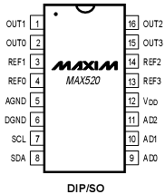
The MAX520 is available in 16-pin DIP and wide SO pack-ages, as well as a space-saving 20-pin SSOP. The MAX521 comes in 20-pin DIP and 24-pin SO packages, as well as a space-saving 24-pin SSOP.

 MAX520 Data Sheet


