Features: ±1 LSB INL
1µA Shutdown Current
"Glitch Free" Output Voltage at Power-Up
Single-Supply Operation
+5V (MAX5174)
+3V (MAX5176)
Full-Scale Output Range
+2.048V (MAX5176, VREF= +1.25V)
+4.096V (MAX5174, VREF= +2.5V )
Rail-to-Rail ® Output Amplifier
Adjustable Output Offset
Low THD (-80dB) in Multiplying Operation
SPI/QSPI/MICROWIRE-Compatible 3-Wire Serial
Interface
Programmable Shutdown Mode and Power-Up
Reset
Buffered Output Capable of Driving 5kΩ|| 100pF
Loads
User-Programmable Digital Output Pin Allows
Serial Control of External Components
14-Bit Upgrades Available (MAX5170/MAX5172)ApplicationIndustrial Process Controls
Digital Offset and Gain Adjustment
Motion Control
Automatic Test Equipment (ATE)
Remote Industrial Controls
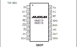
µP-Controlled SystemsPinout Specifications
VDD to AGND, DGND...............................................-0.3V to +6.0V
AGND to DGND.......................................................-0.3V to +0.3V
Digital Inputs to DGND...........................................-0.3V to +6.0V
DOUT, UPO to DGND.....................................-0.3V to (VDD+ 0.3V)
OUT, REF to AGND .......................................-0.3V to (VDD+ 0.3V)
OS to AGND ....................................(AGND - 4.0V) to (VDD+ 0.3V)
Maximum Current into Any Pin.............................................50mA
Continuous Power Dissipation (TA= +70°C)
16-Pin QSOP (derate 8mW/°C above +70°C)...................667mW
Operating Temperature Range............................-40°C to +85°C
Storage Temperature Range.............................-65°C to +150°C
Lead Temperature (soldering, 10sec)..............................+300°C
Stresses beyond those listed under "Absolute Maximum Ratings" may cause permanent damage to the device. These are stress ratings only, and functional operation of the device at these or any other conditions beyond those indicated in the operational sections of the specifications is not implied. Exposure to absolute maximum rating conditions for extended periods may affect device reliability.
DescriptionThe MAX5174/MAX5176 low-power, serial, voltage-out-put, 12-bit digital-to-analog converters (DACs) feature a precision output amplifier in a space-saving 16-pin QSOP package. The MAX5174 operates from a single +5V supply, and the MAX5176 operates from a single +3V supply. Both devices draw only 280µA of supply current, which reduces to 1µA in shutdown. In addition, the programmable power-up reset feature allows for a user-selectable output voltage state of either 0 or midscale.
The 3-wire, digital, serial interface of MAX5174 is compatible with SPI™/QSPI™, and MICROWIRE™ standards. An input register followed by a DAC register provides a double buffered input, allowing the input and DAC registers to be updated independently or simultaneously with a 16-bit serial word. Additional features include software and hardware shutdown, shutdown lockout, a hardware clear pin, and a reference input capable of accepting DC and offset AC signals. The MAX5174 provides a programmable digital output pin for added functionality and a serial-data output pin for daisy-chaining. All logic inputs are TTL/CMOS compatible and are internally buffered with Schmitt triggers to allow direct interfacing to optocouplers.
The MAX5174/MAX5176 incorporate a proprietary on chip circuit that keeps the output voltage virtually"glitch free," limiting the glitches to a few millivolts during power-up. Both devices are available in 16-pin QSOP packages and are specified for the extended (-40°C to +85°C) temperature range. The MAX5170/MAX5172 are pincompatible 14-bit upgrades to the MAX5174/MAX5176.
For 100% pin-compatible DACs with internal reference, see the 13-bit MAX5130/MAX5131 and the 12-bit MAX5120/MAX5121 data sheets.

 MAX5174 Data Sheet


