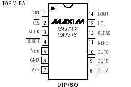
Features: © Operate from a Single +5V (MAX512) or +3V (MAX513) Supply, or from Bipolar Supplies
© Low Power Consumption 1mA Operating Current <1µA Shutdown Current
© Unipolar or Bipolar Outputs
© 5MHz, 3-Wire Serial Interface
© SPI, QSPI, and Microwire Compatible
© Two Buffered, Bipolar-Output DACs (DACs A/B)
© Independently Programmable Shutdown Mode
© Space-Saving 14-Pin SO/DIP PackagesApplicationDigital Gain and Offset Adjustment
Programmable Attenuators
Programmable Current Sources
Programmable Voltage Sources
RF Digitally Adjustable Bias Circuits
VCO TuningPinout Specifications
VDD to GND ................................................................ -0.3V, +6V
VSS to GND................................................................. -6V, +0.3V
VDD to VSS ................................................................ -0.3V, +12V
Digital Inputs and Outputs to GND............... -0.3V, (VDD + 0.3V)
REFAB ................................................ (VSS - 0.3V), (VDD + 0.3V)
OUTA, OUTB (Note 1)....................................................VSS, VDD
OUTC.............................................................-0.3V, (VDD + 0.3V)
REFC..............................................................-0.3V, (VDD + 0.3V)
Continuous Power Dissipation (TA = +70°C)
Plastic DIP (derate 10.00mW/°C above +70°C) ............800mW
SO (derate 8.33mW/°C above +70°C)...........................667mW
CERDIP (derate 9.09mW/°C above +70°C)...................727mW
Operating Temperature Ranges
MAX51_C_ _ .........................................................0°C to +70°C
MAX51_E_ _.......................................................-40°C to +85°C
MAX51_MJD....................................................-55°C to +125°C
Storage Temperature Range .............................-65°C to +165°C
Lead Temperature (soldering, 10sec) .............................+300°C
Note 1: The outputs may be shorted to VDD, VSS, or GND if the package power dissipation is not exceeded. Typical short-circuit current to GND is 50mA.


Description

The MAX512/MAX513 contain three 8-bit, voltage-output digital-to-analog converters (DAC A, DAC B, and DAC C). Output buffer amplifiers for DACs A and B provide voltage outputs while reducing external component count. The output buffer for DAC A can source or sink 5mA to within 0.5V of VDD or VSS.

The buffer for DAC B can source or sink 0.5mA to within 0.5V of VDD or VSS. DAC C is unbuffered, providing a third voltage output with increased accuracy. The MAX512 operates with a single +5V ±10% supply, and the MAX513 operates with a +2.7V to +3.6V supply. Both devices can also operate with split supplies. The 3-wire serial interface has a maximum operating frequency of 5MHz and is compatible with SPI™, QSPI™, and Microwire™.

The serial input shift register of MAX513 is 16 bits long and consists of 8 bits of DAC input data and 8 bits for DAC selection and shutdown. DAC registers can be loaded independently or in parallel at the positive edge of C - S  . A latched logic output is also available for auxiliary control. Ultra-low power consumption and small packages (14-pin DIP/SO) make the MAX512/MAX513 ideal for portable and battery-powered applications. Supply current is only 1mA, dropping to less than 1µA in shutdown. Any of the three DACs can be independently shut down. In shutdown mode, the DAC's R-2R ladder network is disconnected from the reference input, minimizing system power consumption.

 MAX513 Data Sheet


