VDD to DGND.........................................................................................-0.3V, +6V
20-Pin Plastic DIP (derate 11.11mW/ above +70)................................889mW
VDD to AGND........................................................................................ -0.3V, +6V
20-Pin Wide SO (derate 10.00mW/ above +70)...................................800mW
VSS to DGND.........................................................................................-6V, +0.3V
20-Pin SSOP (derate 10.00mW/ above +70).......... .. .. ......................800mW
VSS to AGND........................................................................................-6V, +0.3V
20-Pin CERDIP (derate 11.11mW/ above +70)...................................889mW
VDD to VSS........................................................................................-0.3V, +12V
Operating Temperature Ranges:
Digital Input Voltage to DGND..................... .. .. ...................-0.3V, (VDD + 0.3V)
MAX5_ _ _C_ _................................................................................0 to +70
REF_............................................................................(VSS - 0.3V), (VDD + 0.3V)
MAX5_ _ _E_ _.............................................................................-40 to +85
OUT_....................................................................................................VDD, VSS
MAX5_ _ _MJ_.............................................................................-55 to +125
Maximum Current into Any Pin...................................................................50mA
Storage Temperature Range......................................................-65 to +150
Continuous Power Dissipation (TA = +70)
Lead Temperature (soldering, 10sec).....................................................+300
16-Pin Plastic DIP (derate 10.53mW/ above +70)...........................842mW
16-Pin Wide SO (derate 9.52mW/ above +70)................................762mW
16-Pin CERDIP (derate 10.00mW/ above +70)................................800mW
Note: The outputs may be shorted to V , V , or AGND if the package power dissipation is not exceeded. Typical short-circuitcurrent
DD SS to AGND is 50mA. Do not bias AGND more than +1V above DGND, or more than 2.5V below DGND.
The MAX509/MAX510 are quad, serial-input, 8-bit volt-age-output digital-to-analog converters (DACs). They operate with a single +5V supply or dual ±5V supplies.Internal, precision buffers swing rail-to-rail. The refer-ence input range includes both supply rails.
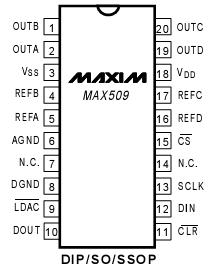
The MAX509 has four separate reference inputs, allow-ing each DAC's full-scale range to be set independently. 20-pin DIP, SSOP, and SO packages are available. The MAX510 is identical to the MAX509 except it has two ref-erence inputs, each shared by two DACs. The MAX510 is housed in space-saving 16-pin DIP and SO packages.
The serial interface of MAX510 is double-buffered: A 12-bit input shift register is followed by four 8-bit buffer registers and four 8-bit DAC registers. A 12-bit serial word is used toload data into each register. Both input and DAC regis-ters can be updated independently or simultaneously with single software commands. Two additional asyn-chronous control pins provide simultaneous updating (LDAC) or clearing (CLR) of input and DAC registers.
TM
The interface of MAX510 is compatible with Microwire and SPI/QSPI TM. All digital inputs and outputs are TTL/CMOS compatible. A buffered data output provides for read-
back or daisy-chaining of serial devices.

 MAX510 Data Sheet


