MAX5090C

Features: · Wide Input Voltage Range: 6.5V to 76V· Fixed (3.3V, 5V) and Adjustable (1.265V to 11V)Output-Voltage Versions· 2A Output Current· Efficiency Up to 92%· Internal 0.26Ω High-Side DMOS FET· 310µA Quiescent Current at No Load· 19µA Shutdown Current· Internal Frequency Com...

product image

MAX5090C Picture
SeekIC No. : 004411083 Detail

MAX5090C: Features: · Wide Input Voltage Range: 6.5V to 76V· Fixed (3.3V, 5V) and Adjustable (1.265V to 11V)Output-Voltage Versions· 2A Output Current· Efficiency Up to 92%· Internal 0.26Ω High-Side DMO...

floor Price/Ceiling Price

Part Number:
MAX5090C
Supply Ability:
5000

Price Break

  • Qty
  • 1~5000
  • Unit Price
  • Negotiable
  • Processing time
  • 15 Days
Total Cost: $ 0.00

SeekIC Buyer Protection PLUS - newly updated for 2013!

  • Escrow Protection.
  • Guaranteed refunds.
  • Secure payments.
  • Learn more >>

Month Sales

268 Transactions

Rating

evaluate  (4.8 stars)

Upload time: 2024/11/27

Payment Methods

All payment methods are secure and covered by SeekIC Buyer Protection PLUS.

Notice: When you place an order, your payment is made to SeekIC and not to your seller. SeekIC only pays the seller after confirming you have received your order. We will also never share your payment details with your seller.
Product Details

Description


Features:

· Wide Input Voltage Range: 6.5V to 76V
· Fixed (3.3V, 5V) and Adjustable (1.265V to 11V)
Output-Voltage Versions
· 2A Output Current
· Efficiency Up to 92%
· Internal 0.26Ω High-Side DMOS FET
· 310µA Quiescent Current at No Load
· 19µA Shutdown Current
· Internal Frequency Compensation
· Fixed 127kHz Switching Frequency
· External Frequency Synchronization
· Thermal Shutdown and Short-Circuit Current Limit
· -40°C to +125°C Automotive Temperature Range
· 16-Pin (5mm x 5mm) Thin QFN Package
· Capable of Dissipating 2.67W at +70°C


Application

·Automotive
·Industrial
·Distributed Power


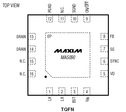
Pinout

  Connection Diagram


Specifications

(Voltages referenced to PGND, unless otherwise specified.)
VIN, DRAIN ..............................................................-0.3V to +80V
SGND, PGND...........................................................-0.3V to +0.3V
LX.................................................................-0.8V to (VIN + 0.3V)
BST ...............................................................-0.3V to (VIN + 10V)
BST to LX................................................................-0.3V to +10V
ON/OFF........................................................-0.3V to (VIN + 0.3V)
VD, SYNC ...............................................................-0.3V to +12V
SS..............................................................................-0.3 to +4V
FB
MAX5090A/MAX5090B...........................................-0.3V to +15V
MAX5090C.....................1mA (internally clamped to +2V, -0.3V)
VOUT Short-Circuit Duration.....................................Continuous
VD Short-Circuit Duration.........................................Continuous
Continuous Power Dissipation (TA = +70°C)*
16-Pin TQFN (derate 33.3mW/°C above +70°C) ........2.667W
Operating Junction Temperature Range.......-40°C to +125°C
Storage Temperature Range .......................-65°C to +150°C
Junction Temperature..................................................+150°C
Lead Temperature (soldering, 10s) ............................+300°C
*As per JEDEC 51 Standard Multilayer Board.


Description

The MAX5090C easy-to-use, high-efficiency, highvoltage step-down DC-DC converters operate from an input voltage up to 76V, and consume only 310µA quiescent current at no load. This pulse-width-modulated (PWM) converter operates at a fixed 127kHz switching frequency at heavy loads, and automatically switches to pulse-skipping mode to provide low quiescent current and high efficiency at light loads. The MAX5090C includes internal frequency compensation simplifying circuit implementation. The device can also be synchronized with external system clock frequency in a noise-sensitive application. The MAX5090C uses an internal low on-resistance and a high-voltage DMOS transistor to obtain high efficiency and reduce overall system cost. This device includes undervoltage lockout, cycle-by-cycle current limit, hiccup-mode output short-circuit protection, and overtemperature shutdown.

The MAX5090C delivers up to 2A output current. External shutdown is included, featuring 19µA (typ) shutdown current. The MAX5090A/MAX5090B versions have fixed output voltages of 3.3V and 5V, respectively, while the MAX5090C features an adjustable 1.265V to 11V output voltage.

The MAX5090C is available in a space-saving 16-pin thin QFN package (5mm x 5mm) and operates over the automotive temperature range (-40°C to +125°C).


Customers Who Bought This Item Also Bought

Margin,quality,low-cost products with low minimum orders. Secure your online payments with SeekIC Buyer Protection.
Programmers, Development Systems
Integrated Circuits (ICs)
Semiconductor Modules
LED Products
Crystals and Oscillators
View more