MAX5089

Features: ·4.5V to 5.5V or 5.5V to 23V Input Voltage Range·Output Voltage Adjustable Down to 0.6V·2A Output Current·Synchronous Rectifier Driver Output (MAX5089) for Higher Efficiency·Resistor-Programmable Switching Frequency from 200kHz to 2.2MHz·External Synchronization and Enable (On/Off) Input...

product image

MAX5089 Picture
SeekIC No. : 004411079 Detail

MAX5089: Features: ·4.5V to 5.5V or 5.5V to 23V Input Voltage Range·Output Voltage Adjustable Down to 0.6V·2A Output Current·Synchronous Rectifier Driver Output (MAX5089) for Higher Efficiency·Resistor-Progr...

floor Price/Ceiling Price

Part Number:
MAX5089
Supply Ability:
5000

Price Break

  • Qty
  • 1~5000
  • Unit Price
  • Negotiable
  • Processing time
  • 15 Days
Total Cost: $ 0.00

SeekIC Buyer Protection PLUS - newly updated for 2013!

  • Escrow Protection.
  • Guaranteed refunds.
  • Secure payments.
  • Learn more >>

Month Sales

268 Transactions

Rating

evaluate  (4.8 stars)

Upload time: 2024/11/27

Payment Methods

All payment methods are secure and covered by SeekIC Buyer Protection PLUS.

Notice: When you place an order, your payment is made to SeekIC and not to your seller. SeekIC only pays the seller after confirming you have received your order. We will also never share your payment details with your seller.
Product Details

Description


Features:

·4.5V to 5.5V or 5.5V to 23V Input Voltage Range
·Output Voltage Adjustable Down to 0.6V
·2A Output Current
·Synchronous Rectifier Driver Output (MAX5089) for Higher Efficiency
·Resistor-Programmable Switching Frequency from 200kHz to 2.2MHz
·External Synchronization and Enable (On/Off) Inputs
·Clock Output for Driving Second Converter 180° Out-Of-Phase (MAX5089)
·Integrated 150mΩ High-Side n-Channel Power MOSFET
·Power-On Reset Output (MAX5088)/Power-Good Output (MAX5089)
·Short-Circuit Protection
·Thermal-Shutdown Protection
·Thermally Enhanced 16-Pin TQFN Package Dissipates 2.7W


Application

·xDSL Modem Power Supply
·Automotive Radio Power Supply
·Servers and Networks
·IP Phones/WLAN Access Points


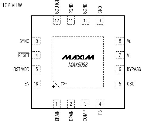
Pinout

  Connection Diagram


Specifications

V+ to PGND............................................................-0.3V to +25V
BST/VDD, DRAIN to SGND .....................................-0.3V to +30V
SGND to PGND .....................................................-0.3V to +0.3V
BST/VDD to SOURCE...............................................-0.3V to +6V
SOURCE to SGND..................................................-0.6V to +25V
SOURCE or DRAIN Maximum Peak Current................5A for 1ms
VL to SGND ..............-0.3V to the lower of +6V and (V+ + 0.3V)
SYNC, EN, DL, CKO, OSC, COMP,
FB to SGND.................................................-0.3V to (VL + 0.3V)
BYPASS, CKO, OSC, COMP, FB, EN, SYNC, RESET,
PGOOD Maximum Input Current ...................................±50mA
RESET, PGOOD to SGND .......................................-0.3V to +6V
BYPASS to SGND.................................................-0.3V to +2.2V
VL and BYPASS Short-Circuit Duration to SGND ......Continuous
Continuous Power Dissipation* (TA = +70°C)
16-Pin TQFN (derate 33mW/°C above +70°C) .........2666mW
Package Thermal Resistance (junction to case) .........1.7°C/W
Operating Temperature Range ....................-40°C to +125°C
Junction Temperature Range .......................-65°C to +150°C
Storage Temperature Range .............................-65°C to +150°C
Lead Temperature (soldering, 10s) .................................+300°C
*As per JEDEC51 Standard (multilayer board).


Description

The MAX5088/MAX5089 high-frequency, DC-DC converters with an integrated n-channel power MOSFET provide up to 2A of load current. The MAX5088 includes an internal power MOSFET to enable the design of a nonsynchronous buck topology power supply. The MAX5089 is for the design of a synchronous buck topology power supply. These devices operate from a 4.5V to 5.5V or 5.5V to 23V input voltage and a 200kHz to 2.2MHz resistor-programmable switching frequency. The voltage-mode architecture with a peak switch current-limit scheme provides stable operation up to a 2.2MHz switching frequency. The MAX5088 includes a clock output for driving a second DC-DC converter 180° out-of-phase and a power-on-reset (RESET) output. The MAX5089 includes a power-good output and a synchronous rectifier driver to drive an external low-side MOSFET in the buck converter configuration for high efficiency.

The MAX5088/MAX5089 protect against overcurrent conditions by utilizing a peak current limit as well as overtemperature shutdown providing a very reliable and compact power source for point-of-load regulation applications. Additional features include synchronization, internal digital soft-start, and an enable input. The MAX5088/MAX5089 are available in a thermally enhanced, space-saving 16-pin TQFN (5mm x 5mm) package and operate over the -40°C to +125°C temperature range.


Customers Who Bought This Item Also Bought

Margin,quality,low-cost products with low minimum orders. Secure your online payments with SeekIC Buyer Protection.
Transformers
Hardware, Fasteners, Accessories
Cables, Wires
Audio Products
Potentiometers, Variable Resistors
Programmers, Development Systems
View more