Features: 4V to 15V Single Power Supply
4A Peak Source/Sink Drive Current
20ns (typ) Propagation Delay
Matching Delay Between Inverting and Noninverting Inputs
Matching Propagation Delay Between Two Channels
VDD / 2 CMOS Logic Inputs (MAX5054AATA)
TTL Logic Inputs (MAX5054B/MAX5055/MAX5056/MAX5057)
0.1 x VDD (CMOS) and 0.3V (TTL) Logic-Input Hysteresis
Up to +18V Logic Inputs (Regardless of VDD Voltage)
Low Input Capacitance: 2.5pF (typ)
40A (typ) Quiescent Current
-40°C to +125°C Operating Temperature Range
8-Pin TDFN and SO PackagesApplicationPower MOSFET Switching Motor Control
Switch-Mode Power Supplies Power-Supply Modules
DC-DC ConvertersPinout Specifications(Voltages referenced to GND.)
VDD.............................................................................-0.3V to +18V
INA+, INA-, INB+, INB-...............................................-0.3V to +18V
OUTA, OUTB ...................................................-0.3V to (VDD + 0.3V)
OUTA, OUTB Short-Circuit Duration........................................10ms
Continuous Source/Sink Current at OUT_ (PD < PDMAX).....200mA
Continuous Power Dissipation (TA = +70°C)
8-Pin TDFN-EP (derate 24.4mW/°C above +70°C)........1951mW
Junction-to-Case Thermal Resistance (JC)......................2°C/W
8-Pin SO-EP (derate 19.2mW/°C above +70°C).........1538mW
Junction-to-Case Thermal Resistance (JC)......................6°C/W
8-Pin SO (derate 5.9mW/°C above +70°C)...................471mW
Junction-to-Case Thermal Resistance (JC)....................40°C/W
Operating Temperature Range..............................-40°Cto +125°C
Storage Temperature Range.................................-65°C to +150°C
Junction Temperature...........................................................+150°C
Lead Temperature (soldering, 10s)......................................+300°CDescriptionThe MAX5054MAX5057 dual, high-speed MOSFET drivers source and sink up to 4A peak current. These devices feature a fast 20ns propagation delay and 20ns rise and fall times while driving a 5000pF capacitive load. Propagation delay time is minimized and matched between the inverting and noninverting inputs and between channels. High sourcing/sinking peak cur-rents, low propagation delay, and thermally enhanced packages make the MAX5054-MAX5057 ideal for high-frequency and high-power circuits.
The MAX5054MAX5057 operate from a 4V to 15V single power supply and consume 40A (typ) of supply current when not switching. These devices have internal logic circuitry that prevents shoot-through during output state changes to minimize the operating current at high switching frequency. The logic inputs are protected against voltage spikes up to +18V, regardless of the V
DD voltage. The MAX5054A is the only version that has CMOS input logic levels while the MAX5054B/MAX5055/MAX5056/MAX5057 have TTL input logic levels.
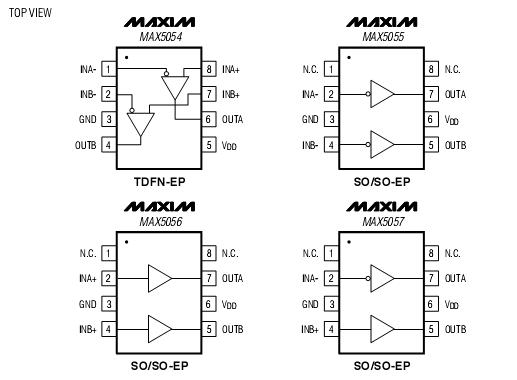
The MAX5055MAX5057 provide the combination of dual inverting, dual noninverting, and inverting/noninverting input drivers. The MAX5054 feature both inverting and noninverting inputs per driver for greater flexibility. They are available in 8-pin TDFN (3mm x 3mm), standard SO,and thermally enhanced SO packages. These devices operate over the automotive temperature range of -40°C to +125°C.

 MAX5057 Data Sheet


