Features: 4V to 15V Single Power Supply
4A Peak Source/Sink Drive Current
20ns (typ) Propagation Delay
Matching Delay Between Inverting and Noninverting Inputs
Matching Propagation Delay Between Two Channels
VDD / 2 CMOS Logic Inputs (MAX5054AATA)
TTL Logic Inputs (MAX5054B/MAX5055/MAX5056/MAX5057)
0.1 x VDD (CMOS) and 0.3V (TTL) Logic-Input Hysteresis
Up to +18V Logic Inputs (Regardless of VDD Voltage)
Low Input Capacitance: 2.5pF (typ)
40A (typ) Quiescent Current
-40°C to +125°C Operating Temperature Range
8-Pin TDFN and SO PackagesApplicationPower MOSFET Switching Motor Control
Switch-Mode Power Supplies Power-Supply Modules
DC-DC ConvertersPinout Specifications(Voltages referenced to GND.)
VDD.............................................................................-0.3V to +18V
INA+, INA-, INB+, INB-...............................................-0.3V to +18V
OUTA, OUTB ...................................................-0.3V to (VDD + 0.3V)
OUTA, OUTB Short-Circuit Duration........................................10ms
Continuous Source/Sink Current at OUT_ (PD < PDMAX).....200mA
Continuous Power Dissipation (TA = +70°C)
8-Pin TDFN-EP (derate 24.4mW/°C above +70°C)........1951mW
Junction-to-Case Thermal Resistance (JC)......................2°C/W
8-Pin SO-EP (derate 19.2mW/°C above +70°C).........1538mW
Junction-to-Case Thermal Resistance (JC)......................6°C/W
8-Pin SO (derate 5.9mW/°C above +70°C)...................471mW
Junction-to-Case Thermal Resistance (JC)....................40°C/W
Operating Temperature Range..............................-40°Cto +125°C
Storage Temperature Range.................................-65°C to +150°C
Junction Temperature...........................................................+150°C
Lead Temperature (soldering, 10s)......................................+300°CDescriptionThe MAX5055 dual, high-speed MOSFET drivers source and sink up to 4A peak current. These devices feature a fast 20ns propagation delay and 20ns rise and fall times while driving a 5000pF capacitive load. Propagation delay time is minimized and matched between the inverting and noninverting inputs and between channels. High sourcing/sinking peak cur-rents, low propagation delay, and thermally enhanced packages make the MAX5055 ideal for high-frequency and high-power circuits.
The MAX5055 operate from a 4V to 15V single power supply and consume 40A (typ) of supply current when not switching. The MAX5055 has internal logic circuitry that prevents shoot-through during output state changes to minimize the operating current at high switching frequency. The logic inputs are protected against voltage spikes up to +18V, regardless of the V
DD voltage. The MAX5054A is the only version that has CMOS input logic levels while the MAX5055 has TTL input logic levels.
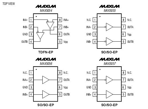
The MAX5055 provide the combination of dual inverting, dual noninverting, and inverting/noninverting input drivers. The MAX5054 feature both inverting and noninverting inputs per driver for greater flexibility. They are available in 8-pin TDFN (3mm x 3mm), standard SO,and thermally enhanced SO packages. The MAX5055 operate over the automotive temperature range of -40°C to +125°C.

 MAX5055 Data Sheet


