Features: ` 2mm *2mm UCSP
` Guaranteed On-Resistance (RON)
25 (max) at +5V
50 (max) at +3V
` On-Resistance Matching
3 (max) at +5V
3.5 (max) at +3V
` Guaranteed <0.1nA Leakage Current at TA = +25°C
` Single-Supply Operation from +2.0V to +11V
` TTL/CMOS-Logic Compatible
` -84dB Crosstalk (1MHz)
` -72dB Off-Isolation (1MHz)
` Low Power Consumption: 0.5nW (typ)
` Rail-to-Rail Signal HandlingApplication·Battery-Powered Systems
·Audio/Video-Signal Routing
·Low-Voltage Data-Acquisition Systems
·Cell Phones
·Communications Circuits
·Glucose Meters
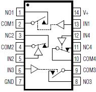
·PDAsPinout
Specifications(All voltages referenced to GND)
V+............................................................................-0.3V to +12V
IN_, COM_, NO_, NC_ (Note 1).......................-0.3V to (V+ + 0.3V)
Continuous Current (any pin) ...........................................±10mA
Peak Current (any pin, pulsed at 1ms, 10% duty cycle) ...±20mA
Continuous Power Dissipation (TA = +70°C)
14-Pin TSSOP (derate 6.3mW/°C above +70°C) ...........500mW
16-Bump UCSP (derate 8.3mW/°C above +70°C) .........659mW
Operating Temperature Range .........................-40°C to +85°C
Storage Temperature Range ..........................-65°C to +150°C
Maximum Junction Temperature .....................................+150°C
Bump Temperature (soldering, Note 2)
Infrared (15s) ................................................................+220°C
Vapor Phase (60s) .........................................................+215°C
Lead Temperature (soldering, 10s) ................................+300°C
Note 1: Signals on IN_, NO_, NC_, or COM_ exceeding V+ or GND are clamped by internal diodes. Limit forward-diode current to maximum current rating.
Note 2: This device is constructed using a unique set of packaging techniques that impose a limit on the thermal profile the device can be exposed to during board-level solder attach and rework. This limit permits only the use of the solder profiles recommended in the industry-standard specification, JEDEC 020A, paragraph 7.6, Table 3 for IR/VPR and convection reflow. Preheating is required. Hand or wave soldering is not allowed.
Stresses beyond those listed under "Absolute Maximum Ratings" may cause permanent damage to the device. These are stress ratings only, and functional operation of the device at these or any other conditions beyond those indicated in the operational sections of the specifications is not implied. Exposure to absolute maximum rating conditions for extended periods may affect device reliability
DescriptionThe MAX4749 low-voltage, quad single-pole single-throw (SPST)/dual single-pole/double-throw (SPDT) analog switches operate from a single +2V to +11V supply and handle Rail-to-Rail® analog signals. These switches exhibit low leakage current (0.1nA) and consume less than 0.5nW (typ) of quiescent power, making them ideal for battery-powered applications.
When powered from a +3V supply, the MAX4749 feature 50 (max) on-resistance (RON), with 3.5 (max) matching between channels and 9 (max) flatness over the specified signal range.
The MAX4747 has four normally open (NO) switches, the MAX4748 has four normally closed (NC) switches, and the MAX4749 has two NO and two NC switches. The MAX4750 has two SPDT switches. These switches are available in 14-pin TSSOP and 16-bump chip-scale packages (UCSP™). This tiny chip-scale package occupies a 2mm * 2mm area and significantly reduces the required PC board area.

 MAX4749 Data Sheet


