Features: No Power-Supply Sequencing Required
All Channels Off with Power Off
Rail-to-Rail Signal Handling
400 (max) On-Resistance
±40V Fault Protection with Power Off
±25V Fault Protection with ±15V Supplies
100ns Fault-Response Time
±4.5V to ±20V Dual Supplies
+9V to +36V Single Supply
TTL/CMOS-Compatible Logic Inputs
ApplicationData-Acquisition Systems Industrial and Process Control Avionics Signal Routing Redundancy/Backup Systems ATE Systems Hot Swap
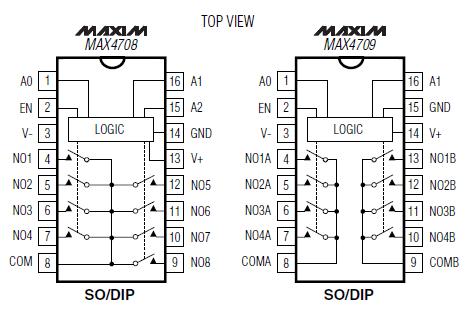
Pinout Specifications
(All Voltages Referenced to GND)
V+...................................................................................-0.3V to +44.0V
V- ...................................................................................-44.0V to +0.3V
V+ to V-..........................................................................-0.3V to +44.0V
COM_, A_, EN (Note 1).................................... (V+ + 0.3V) to (V- - 0.3V)
NO_....................................................................(V+ - 40V) to (V- + 40V)
NO_ to COM_ .....................................................................-36V to +36V
NO_ Voltage with Switch Power On ...................................-30V to +30V
NO_ Voltage with Switch Power Off ...................................-40V to +40V
Continuous Current into any Terminal. ........................................±30mA
Peak Current into any Terminal
(pulsed at 1ms, 10% duty cycle).................................................±100mA
Continuous Power Dissipation (TA = +70°C)
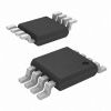
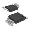
16 Narrow SO (derate 8.70mW/°C above +70°C) .....................696mW
16 Plastic DIP (derate 10.53mW/°C above +70°C) ....................842mW
16 Wide SO (derate 9.52mW/°C above +70°C)..........................762mW
Operating Temperature Range
MAX4708E_ E/MAX4709E_E ...........................................-40°C to +85°C
Junction Temperature.................................................................. +150°C
Storage Temperature Range ........................................-65°C to +160°C
Lead Temperature (soldering, 10s) ..............................................+300°C
Note 1: COM_, EN, and A_ pins are not fault protected. Signals on COM_, EN, or A_ exceeding V+ or V- are clamped by internal diodes. Limit forward-diode current to maximum current rating.
DescriptionThe MAX4708/MAX4709 8-to-1 and dual 4-to-1 fault-protected multiplexers are pin compatible with the industrystandard DG508/DG509. The MAX4708/MAX4709 are similar to the MAX4508/MAX4509, but these devices do not have clamp diodes to the supply rails on the switch outputs. These multiplexers feature fault-protected inputs, Rail-to-Rail® signal-handling capability, and do not require power-supply sequencing.
Both devices offer ±40V overvoltage protection with the supplies off, ±36V protection with the supplies on, and feature 400 (max) on-resistance with 15 (max) matching between channels. The MAX4708/MAX4709 operate with dual supplies of ±4.5V to ±20V or a single supply of +9V to +36V. All digital inputs have TTL logiccompatible thresholds, ensuring both TTL and CMOS logic compatibility when using a single +12V supply or dual ±15V supplies.
For low-voltage applications requiring fault protection, refer to the MAX4709 data sheet.

 MAX4709 Data Sheet


