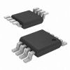
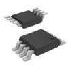
Features: ` Tiny UCSP (1.5mm x 1.5mm)
` Drives 120mW into 16
` 0.03% THD + N at 1kHz
` 2.3V to 5.5V Single-Supply Operation
` 1mA Supply Current Per Amplifier
` Very High Power-Supply Rejection Ratio (96dB)
` Unity-Gain Stable
` Rail-to-Rail Output Stage
` Thermal Overload and Short-Circuit ProtectionApplication·Cellular Phones
·Headphones
·Headsets
·PDAs
·DC Motor Control
·General-Purpose AudioSpecificationsVCC to GND.............................................................-0.3V to +6V
All Other Pins to GND.................................-0.3V to (VCC + 0.3V)
Output Short Circuit to VCC or GND (Note 1)............Continuous
Continuous Power Dissipation (TA = +70°C)
9-Bump USCP (derate 4.7mW/°C above +70°C).........379mW
Operating Temperature Range ......................-40°C to +85°C
Junction Temperature...................................................+150°C
Storage Temperature Range .......................-65°C to +150°C
Bump Temperature (soldering) (Note 2)
Infrared (15s) ..............................................................+220°C
Vapor Phase (60s) .......................................................+215°C
Note 1: Continuous power dissipation must also be observed.
Note 2: This device is constructed using a unique set of packaging techniques that impose a limit on the thermal profile that the device can be exposed to during board-level solder attach and rework. This limit permits only the use of the solder profiles recommended in the industry standard specification, JEDEC 020A, paragraph 7.6, Table 3 for IR/VPR and convection reflow. Preheating is required. Hand or wave soldering is not allowed.
Stresses beyond those listed under "Absolute Maximum Ratings" may cause permanent damage to the device. These are stress ratings only, and functional operation of the device at these or any other conditions beyond those indicated in the operational sections of the specifications is not implied. Exposure to absolute maximum rating conditions for extended periods may affect device reliability.
DescriptionThe MAX4369 dual, high-output-drive op amp combines single-supply operation with high-output-current drive, Rail-to-Rail® outputs in an ultra chip-scale package (UCSP™). The device is unity-gain stable to 3.5MHz and operates from a single 2.3V to 5.5V supply. The MAX4369 is guaranteed to source and sink up to 87mA with a 5V supply.
The MAX4369 is capable of delivering 120mW of continuous average power to a 16 load, or 75mW to a 32 load with 1% total harmonic distortion plus noise (THD + N), making the device ideal for portable audio applications.
The MAX4369 is specified over the extended temperature range (-40°C to +85°C) and is available in a tiny (1.5mm x 1.5mm) 9-bump UCSP.

 MAX4369 Data Sheet


