Features: ` +4.5V to +8.0V Single-Supply Operation` Superior SFDR with 100 Load -90dBc (fC = 5MHz ) -60dBc (fC = 100MHz)` 35dBm IP3 (fC = 20MHz)` 8nV/Hz Voltage Noise Density` 100MHz 0.1dB Gain Flatness (MAX4268)` 900V/s Slew Rate` ±45mA Output Driving Capability` Shutdown Mode Places Outputs in H...
MAX4270: Features: ` +4.5V to +8.0V Single-Supply Operation` Superior SFDR with 100 Load -90dBc (fC = 5MHz ) -60dBc (fC = 100MHz)` 35dBm IP3 (fC = 20MHz)` 8nV/Hz Voltage Noise Density` 100MHz 0.1dB Gain Flat...
SeekIC Buyer Protection PLUS - newly updated for 2013!
268 Transactions
All payment methods are secure and covered by SeekIC Buyer Protection PLUS.
Supply Voltage (VCC to VEE)...............................................+8.5V
Voltage on Any Other Pin ................(VEE - 0.3V) to (VCC + 0.3V)
Short-Circuit Duration (VOUT to VCC or VEE) ..............Continuous
Continuous Power Dissipation (TA = +70°C)
16-Pin QSOP (derate 8.33mW/°C above +70°C)........667mW
8-Pin MAX (derate 4.10mW/°C above +70°C) ..........330mW
8-Pin SO (derate 5.9mW/°C above +70°C).................471mW
14-Pin SO (derate 8.33mW/°C above +70°C).............667mW
Operating Temperature Range ......................-40°C to +85°C
Storage Temperature Range ........................-65°C to +150°C
Junction Temperature...................................................+150°C
Lead Temperature (soldering, 10s) ..............................+300°C
Stresses beyond those listed under "Absolute Maximum Ratings" may cause permanent damage to the device. These are stress ratings only, and functional operation of the device at these or any other conditions beyond those indicated in the operational sections of the specifications is not implied. Exposure to absolute maximum rating conditions for extended periods may affect device reliability.
The MAX4265MAX4270 single-supply, voltage-feedback op amps are capable of driving a 100 load while maintaining ultra-low distortion over a wide bandwidth. They offer superior spurious-free dynamic range (SFDR) performance: -90dBc or better at frequencies below 5MHz and -60dBc at a 100MHz frequency. Additionally, input voltage noise density is 8nV/Hz while operating from a single +4.5V to +8.0V supply or from dual ±2.25V to ±4.0V supplies. These features make the MAX4265MAX4270 ideal for use in high-performance communications and signalprocessing applications that require low distortion and wide bandwidth.
The MAX4265 single and MAX4268 dual unity-gain-stable amplifiers have up to a 300MHz gain-bandwidth product. The MAX4266 single and MAX4269 dual amplifiers have up to a 350MHz bandwidth at a minimum stable gain of +2V/V. The MAX4267 single and MAX4270 dual amplifiers have a 200MHz bandwidth at a minimum stable gain of +5V/V.
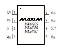
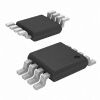
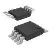
For additional power savings, these amplifiers feature a low-power disable mode that reduces supply current to 1.6mA and places the outputs in a high-impedance state. The MAX4265/MAX4266/MAX4267 are available in a space-saving 8-pin MAX package, and the MAX4268/ MAX4269/MAX4270 are available in a 16-pin QSOP package.