Features: ` Operates from +4.5V to +8.0V
` Superior SFDR with 100 Load
-90dBc (fC = 5MHz )
-59dBc (fC = 100MHz)
` 35dBm IP3 (fC = 20MHz)
` 8nV/Hz Voltage Noise Density
` 100MHz 0.1dB Gain Flatness (MAX4268)
` 900V/s Slew Rate
` ±45mA Output Driving Capability
` Disable Mode Places Outputs in High-Impedance StateApplication·Base-Station Amplifiers
·IF Amplifiers
·High-Frequency ADC Drivers
·High-Speed DAC Buffers
·RF Telecom Applications
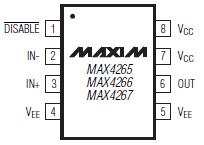
·High-Frequency Signal ProcessingPinout
SpecificationsSupply Voltage (VCC to VEE).............................................+8.5V
Voltage on Any Other Pin ...............(VEE - 0.3V) to (VCC + 0.3V)
Short-Circuit Duration (VOUT to VCC or VEE) ............Continuous
Continuous Power Dissipation (TA = +70°C)
8-Pin MAX (derate 4.10mW/°C above +70°C) ..........330mW
16-Pin QSOP (derate 8.33mW/°C above +70°C)........667mW
8-Pin SO (derate 5.9mW/°C above +70°C).................471mW
14-Pin SO (derate 8.33mW/°C above +70°C).............667mW
Operating Temperature Range ......................-40°C to +85°C
Storage Temperature Range ........................-65°C to +150°C
Junction Temperature...................................................+150°C
Lead Temperature (soldering, 10s) ..............................+300°C
Stresses beyond those listed under "Absolute Maximum Ratings" may cause permanent damage to the device. These are stress ratings only, and functional operation of the device at these or any other conditions beyond those indicated in the operational sections of the specifications is not implied. Exposure to absolute maximum rating conditions for extended periods may affect device reliability.
DescriptionThe MAX4266 ultra-low distortion, voltage-feedback op amps are capable of driving a 100 load while maintaining ultra-low distortion over a wide bandwidth. They offer superior spurious-free dynamic range (SFDR) performance: -90dBc at 5MHz and -59dBc at 100MHz (MAX4269). Additionally, input voltage noise density is 8nV/Hz while operating from a single +4.5V to +8.0V supply or from dual ±2.25V to ±4.0V supplies. These features make the MAX4266 ideal for use in high-performance communications and signal-processing applications that require low distortion and wide bandwidth.
The MAX4265 single and MAX4268 dual amplifiers are unity-gain stable. The MAX4266 single and MAX4269 dual amplifiers are compensated for a minimum stable gain of +2V/V, while the MAX4267 single and MAX4270 dual amplifiers are compensated for a minimum stable gain of +5V/V.
For additional power savings, these amplifiers feature a low-power disable mode that reduces supply current and places the outputs in a high-impedance state. The MAX4265/MAX4266/MAX4267 are available in a spacesaving 8-pin MAX package, and the MAX4268/ MAX4269/MAX4270 are available in a 16-pin QSOP package.

 MAX4266 Data Sheet


