Features: ` -3dB Bandwidth of 330MHz
` 0.1dB Gain Flatness of 150MHz
` 700V/s Slew Rate
` 0.01°/0.01% Differential Phase/Gain
` Low Power: 5.5mA Max
` -92dB Crosstalk and -78dB Off Isolation at 30MHz
` High-Z Outputs when Disabled
` 3pF Input Capacitance
` Ultra-Low Switching Glitch
` On-Board Control LogicApplication·Video-Router and Crosspoint Arrays
·Broadcast/HDTV-Quality Color Signal Multiplexing
·RF and IF Routing
·Graphics Color-Signal Routing
·Telecom Routing
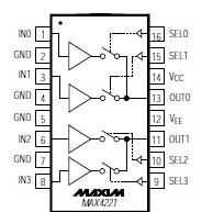
·Data AcquisitionPinout
SpecificationsSupply Voltages
VCC ..................................................................................+6V
VEE ....................................................................................-6V
VCC-VEE ..........................................................................+12V
Analog Input Voltage .......................(VEE - 0.3V) to (VCC + 0.3V)
Digital Input Voltage ..................................-0.3V to (VCC + 0.3V)
Duration of Short Circuit to Ground............................Continuous
Continuous Power Dissipation (TA = +70°C)
8-Pin SO (derate 5.88mW/°C above +70°C)...............471mW
16-Pin Narrow SO (derate 8.70mW/°C above +70°C)...696mW
Operating Temperature Range..............................0°C to +70°C
Storage Temperature Range ...........................-65°C to +160°C
Junction Temperature......................................................+150°C
Lead Temperature (soldering, 10sec) .............................+300°C
Stresses beyond those listed under "Absolute Maximum Ratings" may cause permanent damage to the device. These are stress ratings only, and functional operation of the device at these or any other conditions beyond those indicated in the operational sections of the specifications is not implied. Exposure to absolute maximum rating conditions for extended periods may affect device reliability.
DescriptionThe MAX4111/MAX4121/MAX4221 wideband video switches are optimized for high-definition, broadcastquality,composite (HDTV, NTSC, PAL, SECAM, and RGB) video switching arrays. Their open-loop buffer amplifiers offer 0.1dB gain flatness to 150MHz. They operate from ±5V supplies and feature differential phase and gain error of only 0.01°/0.01%, respectively.The ultra-low switching glitch (13mV) is positive to avoid confusion with any sync pulse.
Ideal as building blocks in large arrays, MAX4111 feature a constant, high input impedance and a disable function that puts the outputs into a high-impedance state and reduces the operating current to only 250A.The open-loop architecture allows the outputs to drive capacitive loads without oscillation. Other key features include -92dB crosstalk and -78dB isolation (MAX4121).
The MAX4111/MAX4121/MAX4221 are offered in narrow plastic DIP and SO packages. See the table below for key features:
|
PART |
DESCRIPTION |
PINS |
| MAX4111 |
SPST, single-input, single-output switch |
8 |
| MAX4121 |
SPDT, 2-input, single-output switch |
8 |
| MAX4221 |
Dual, SPDT, 2-input, single-output switch |
16 |

 MAX4111 Data Sheet


