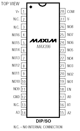
Features: ` Pin Compatible with MAX306/MAX307, DG406/DG407, DG506A/DG507A` Single-Supply Operation (+2.7V to +16V) Dual-Supply Operation (±2.7V to ±8V)` Low On-Resistance (100½ max)` Guaranteed RON Match Between Channels (6 max)` Guaranteed RON Flatness over Specified Signal Range (10 max)`...
MAX396: Features: ` Pin Compatible with MAX306/MAX307, DG406/DG407, DG506A/DG507A` Single-Supply Operation (+2.7V to +16V) Dual-Supply Operation (±2.7V to ±8V)` Low On-Resistance (100½ max)` Guarante...
SeekIC Buyer Protection PLUS - newly updated for 2013!
268 Transactions
All payment methods are secure and covered by SeekIC Buyer Protection PLUS.
(Voltage referenced to GND, unless otherwise noted.)
V+...........................................................................-0.3V to +17V
V- ...........................................................................+0.3V to -17V
V+ to V-..................................................................-0.3V to +17V
Voltage into Any Terminal (Note 1).............(V- - 2V) to (V+ + 2V)
or 30mA (whichever occurs first)
Current into Any Terminal ................................................±30mA
Peak Current into Any Terminal .......................................±50mA
Continuous Power Dissipation (TA = +70°C)
Plastic DIP (derate 14.29mW/°C above +70°C) .........1143mW
Wide SO (derate 12.50mW/°C above +70°C)..............1000mW
SSOP (derate 9.52mW/°C above +70°C) ......................762mW
PLCC (derate 10.53mW/°C above +70°C) ....................842mW
CERDIP (derate 16.67mW/°C above +70°C)...............1333mW
Operating Temperature Ranges
MAX39_C_I ..........................................................0°C to +70°C
MAX39_E_I .......................................................-40°C to +85°C
MAX39_MJI......................................................-55°C to +125°C
Storage Temperature Range ..........................-65°C to +150°C
Lead Temperature (soldering, 10sec) ............................+300°C
Stresses beyond those listed under "Absolute Maximum Ratings" may cause permanent damage to the device. These are stress ratings only, and functional operation of the device at these or any other conditions beyond those indicated in the operational sections of the specifications is not implied. Exposure to absolute maximum rating conditions for extended periods may affect device reliability.
Note 1: Signals on any terminal exceeding V+ or V- are clamped by internal diodes. Limit forward current to maximum current rating.
The MAX396/MAX397 low-voltage, CMOS analog multiplexers (muxes) offer low on-resistance (100 max), which is matched to within 6 between switches and remains flat over the specified signal range (10 max). They also offer low leakage over temperature (input off-leakage current less than 1nA at +85°C) and fast switching speeds (transition time less than 250ns). The MAX396 is a 16-channel device, and the MAX397 is a dual 8-channel device.
The MAX396/MAX397 are fabricated with Maxim's lowvoltage silicon-gate process. Design improvements yield extremely low charge injection (5pC max) and guarantee electrostatic-discharge (ESD) protection greater than 2000V per Method 3015.7 These muxes MAX396 operate with a single +2.7V to +16V supply or with ±2.7V to ±8V dual supplies, while retaining CMOS-logic input compatibility and fast switching.
The MAX396/MAX397 are pin compatible with the industrystandard MAX306/MAX307, DG406/DG407, and DG506A/DG507A.