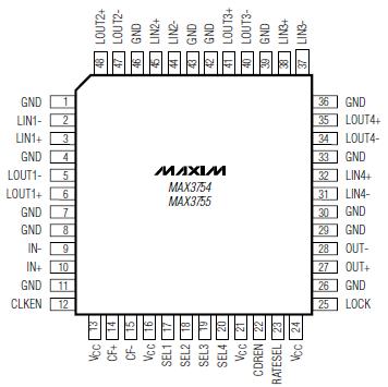
Features: `Pin Selectable 1.0625Gbps/2.125Gbps Dual-Rate Operation
`Meets Fibre Channel Jitter Tolerance
`1400mV Typical Differential Output Swing
`3.0V to 3.6V Operation
`No Reference Clock Required
`Frequency Lock Indication
`1W Power Consumption (MAX3754) at +3.3V
`150 or 100 Differential L-Port Impedance AvailableApplication·1.0625Gbps/2.125Gbps Dual-Rate Fibre Channel
·Fibre Channel Data Storage Systems
·Storage Area Networks
·Fibre Channel HubsPinout Specifications
VCC..........................................................................-0.5V to +5V
Current into OUT±, LOUT1±, LOUT2±,
LOUT3±, LOUT4±.............................................................. 22mA
Voltage at OUT±, LOUT1±, LOUT2±,
LOUT3±, LOUT4±...........................(VCC - 1.65V) to (VCC + 0.5V)
Voltage at IN±, LIN1±, LIN2±, LIN3±,
LIN4±..........................................................-0.5V to (VCC + 0.5V)
Voltage at CLKEN, CF+, CF-, CDREN, RATESEL,
SEL_, LOCK..................................................-0.5V to (VCC + 0.5V)
Current into LOCK.................................................-1mA to +10mA
Continuous Power Dissipation (TA = +70°C)
48-Pin TQFP-EP (derate 30.0mW/°C above +70°C) ..............2W
Operating Junction Temperature Range...........-55°C to +150°C
Operating Temperature Range ........................-55°C to +110°C
Storage Temperature Range ...........................-55°C to +150°C
Lead Temperature (soldering, 10s) .................................+300°C
Stresses beyond those listed under "Absolute Maximum Ratings" may cause permanent damage to the device. These are stress ratings only, and functional operation of the device at these or any other conditions beyond those indicated in the operational sections of the specifications is not implied. Exposure to absolute maximum rating conditions for extended periods may affect device reliability.
DescriptionThe MAX3754 quad-port bypass circuits (PBCs) are designed for use in Fibre Channel Arbitrated Loop applications. Each consists of four serially connected port bypass circuits and a repeater that provides clock and data recovery. The quad-PBC MAX3754 allows connection of up to four Fibre Channel L-ports; each can be enabled or bypassed by individual logic inputs. To reduce the external parts count, all signal inputs and outputs have internal termination resistors. The MAX3754 comply with Fibre Channel jitter tolerance requirements and can recover data signals with up to 0.7 unit intervals (UIs) of high-frequency jitter. These devices operate from a single +3.3V supply.

 MAX3754 Data Sheet


