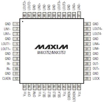
Features: ` Four High-Speed Data Ports` Meets Fibre Channel Jitter Tolerance Requirements` Large Output Signal Swing (>1000mVp-p)` +3.0V to +3.6V Single-Supply Voltage` On-Chip Termination Resistors Compatible with 75 Transmission Lines at All PortsApplication·2.125Gbps Fibre Channel·1.063Gbps ...
MAX3753: Features: ` Four High-Speed Data Ports` Meets Fibre Channel Jitter Tolerance Requirements` Large Output Signal Swing (>1000mVp-p)` +3.0V to +3.6V Single-Supply Voltage` On-Chip Termination Resist...
SeekIC Buyer Protection PLUS - newly updated for 2013!
268 Transactions
All payment methods are secure and covered by SeekIC Buyer Protection PLUS.
The MAX3752/MAX3753 quad-port bypass ICs are designed for use in the Fibre Channel Arbitrated Loop topology. These devices consist of four serially connected port bypass circuits (PBCs) and a repeater that provides clock and data recovery (CDR).
The quad-port bypass circuit of MAX3753 allows connection of up to four Fibre Channel L-Ports, which can each be enabled or bypassed by controlling the PBC select inputs.
Additional quad PBCs of MAX3753 can be cascaded for applications requiring more than four L-Ports. To reduce the external parts count, all signal inputs and outputs have internal termination resistors.
The MAX3752/MAX3753 comply with Fibre Channel jitter tolerance requirements and can recover data signals with up to 0.7 unit intervals (UIs) of high-frequency jitter.
When the repeater is not needed, MAX3753 can be disabled to reduce power consumption. A fully integrated phaselocked loop (PLL) provides a frequency lock indication and does not need an external reference clock.
Two pin-compatible versions of the quad PBC are available- the MAX3752 for 2.125Gbps or 1.063Gbps operation, and the MAX3753 for 1.063Gbps operation.