MAX3672

Features: ·Single +3.3V or +5.0V Supply·Power Dissipation: 150mW at +3.3V Supply·External VCO Center Frequencies (fVCO): 155MHz to 700MHz·Reference Clock Frequencies: fVCO, fVCO/2, fVCO/4, fVCO/8, fVCO/32·Main Clock Output Frequency: fVCO·Optional Output Clock Frequencies: fVCO, fVCO/2, fVCO/4, fV...

product image

MAX3672 Picture
SeekIC No. : 004410117 Detail

MAX3672: Features: ·Single +3.3V or +5.0V Supply·Power Dissipation: 150mW at +3.3V Supply·External VCO Center Frequencies (fVCO): 155MHz to 700MHz·Reference Clock Frequencies: fVCO, fVCO/2, fVCO/4, fVCO/8, f...

floor Price/Ceiling Price

Part Number:
MAX3672
Supply Ability:
5000

Price Break

  • Qty
  • 1~5000
  • Unit Price
  • Negotiable
  • Processing time
  • 15 Days
Total Cost: $ 0.00

SeekIC Buyer Protection PLUS - newly updated for 2013!

  • Escrow Protection.
  • Guaranteed refunds.
  • Secure payments.
  • Learn more >>

Month Sales

268 Transactions

Rating

evaluate  (4.8 stars)

Upload time: 2024/11/27

Payment Methods

All payment methods are secure and covered by SeekIC Buyer Protection PLUS.

Notice: When you place an order, your payment is made to SeekIC and not to your seller. SeekIC only pays the seller after confirming you have received your order. We will also never share your payment details with your seller.
Product Details

Description


Features:

·Single +3.3V or +5.0V Supply
·Power Dissipation: 150mW at +3.3V Supply
·External VCO Center Frequencies (fVCO): 155MHz to 700MHz
·Reference Clock Frequencies: fVCO, fVCO/2, fVCO/4, fVCO/8, fVCO/32
·Main Clock Output Frequency: fVCO
·Optional Output Clock Frequencies: fVCO, fVCO/2, fVCO/4, fVCO/8
·Low Intrinsic Jitter: <0.4psRMS
·Loss-of-Lock Indicator
·PECL Clock Output Interface


Application

·OC-12 to OC-192 SONET/WDM Transport
·Systems
·Clock Jitter Clean-Up and Frequency
·Synchronization
·Frequency Conversion
·System Clock Distribution


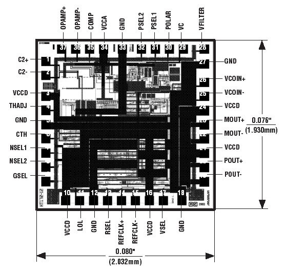
Pinout

  Connection Diagram


Specifications

Supply Voltage ...............................................-0.5V to +7.0V
Voltage at C2+, C2-, THADJ, CTH, NSEL1, NSEL2, GSEL, LOL,
RSEL, REFCLK-, REFCLK+, VSEL, VCOIN+, VCOIN-, VC,
POLAR, PSEL1, PSEL2, COMP,
OPAMP+, OPAMP- ................................-0.5V to (VCC + 0.5V)
Voltage at VFILTER ........................................-0.5V to +3.0V
PECL Output Current (MOUT+,
MOUT-, POUT+, POUT-).................................................56mA
Operating Temperature Range .................-40°C to +85°C
Storage Temperature Range. .................-65°C to +160°C
Die-Attach Process Temperature.............................+400°C
Stresses beyond those listed under "Absolute Maximum Ratings" may cause permanent damage to the device. These are stress ratings only, and functional
operation of the device at these or any other conditions beyond those indicated in the operational sections of the specifications is not implied. Exposure to
absolute maximum rating conditions for extended periods may affect device reliability.


Description

The MAX3672 is a low-jitter 155MHz/622MHz reference clock generator IC designed for system clock distribution and frequency synchronization in OC-48 and OC-192 SONET/SDH and WDM transmission systems. The MAX3672 integrates a phase/frequency detector, an operational amplifier (op amp), prescaler dividers, and input/output buffers. Using an external VCO, the MAX3672 can be configured easily as a phase-lock loop with bandwidth programmable from 30Hz to 10kHz.

The MAX3672 operates from a single +3.3V or +5.0V supply and dissipates 150mW (typ) at 3.3V. The operating temperature range is -40°C to +85°C.


Customers Who Bought This Item Also Bought

Margin,quality,low-cost products with low minimum orders. Secure your online payments with SeekIC Buyer Protection.
Audio Products
Tapes, Adhesives
803
Batteries, Chargers, Holders
Isolators
Sensors, Transducers
LED Products
View more