Features: `±15kV ESD Protection on I/O VCC_ Lines
`Bidirectional Level Translation Without Direction Pin
`I/O VL_ and I/O VCC_ 10mA Sink-/15mA Source-Current Capability
`Slew-Rate Enhancement Circuitry Supports Larger Capacitive Loads or Larger External Pullup Resistors
`6Mbps Push-Pull/1Mbps Open-Drain Guaranteed Data Rate
`Wide Supply-Voltage Range: Operation Down to +1.2V on VL and +1.65V on VCC
`Low Supply Current in Tri-State Output Mode (3A typ)
`Low Quiescent Current
`Thermal-Shutdown Protection
`UCSP, TDFN, and TQFN PackagesApplication·Multivoltage Bidirectional Level Translation
·SPI™, MICROWIRE™, and I2C† Level Translation
·Open-Drain Rise-Time Speed-Up
·High-Speed Bus Fan-Out Expansion
·Cell Phones
·Telecom, Networking, Servers, RAID/SANPinout Specifications
(All voltages referenced to GND.)
VCC .................................................................... -0.3V to +6V
VL ...................................................................... -0.3V to +6V
I/O VCC_ ................................................. -0.3V to VCC + 0.3V
I/O VL_ ...................................................... -0.3V to VL + 0.3V
EN ...................................................................... -0.3V to +6V
Short-Circuit Duration I/O VL_, I/O VCC_ to GND . Continuous
Maximum Continuous Current .................................... ±50mA
Continuous Power Dissipation (TA = +70°C)
8-Pin TDFN (derate 18.2mW/°C above +70°C) ...... 1455mW
9-Bump UCSP (derate 4.7mW/°C above +70°C) ...... 379mW
12-Pin TQFN (derate 16.9mW/°C above +70°C) ..... 1349mW
12-Bump UCSP (derate 6.5mW/°C above +70°C) ..... 519mW
20-Pin TQFN (derate 20.8mW/°C above +70°C) .... .1667mW
20-Bump UCSP (derate 10.0mW/°C above +70°C) ....800mW
Operating Temperature Range ..................... -40°C to +85°C
Storage Temperature Range ...................... -65°C to +150°C
Junction Temperature ..................................................+150°C
Bump Temperature (soldering) ................................... +235°C
Lead Temperature (soldering, 10s) ......................... ... +300°C
Stresses beyond those listed under "Absolute Maximum Ratings" may cause permanent damage to the device. These are stress ratings only, and functional operation of the device at these or any other conditions beyond those indicated in the operational sections of the specifications is not implied. Exposure to absolute maximum rating conditions for extended periods may affect device reliability.
DescriptionThe MAX3394E/MAX3395E/MAX3396E bidirectional level translators provide level shifting required for data transfer in a multivoltage system. Internal slew-rate enhancement circuitry features 10mA current-sink and 15mA current-source drivers to isolate capacitive loads from lower current drivers. In open-drain systems, slewrate enhancement enables fast data rates with larger pullup resistors and increased bus load capacitance. Externally applied voltages, VCC and VL, set the logichigh levels for the device. A logic-low signal on one I/O side of the device appears as a logic-low signal on the opposite I/O side, and vice-versa. Each I/O line is pulled up to VCC or VL by an internal pullup resistor, allowing the devices to be driven by either push-pull or open-drain drivers.
The MAX3394E/MAX3395E/MAX3396E feature a tristate output mode, thermal-shutdown protection, and ±15kV Human Body Model (HBM) ESD protection on the VCC side for greater protection in applications that route signals externally.
The MAX3394E/MAX3395E/MAX3396E accept VCC voltages from +1.65V to +5.5V, and VL voltages from +1.2V to VCC, making them ideal for data transfer between low voltage ASIC/PLDs and higher voltage systems. The MAX3394E/MAX3395E/MAX3396E operate at a guaranteed data rate of 6Mbps with push-pull drivers and 1Mbps with open-drain drivers.
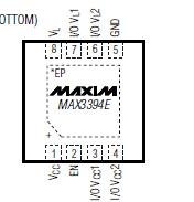
The MAX3394E is a dual-level translator available in 9-bump UCSP™ and 8-pin 3mm x 3mm TDFN packages. The MAX3395E is a quad-level translator available in 12- bump UCSP, and 12-pin 4mm x 4mm TQFN packages. The MAX3396E is an octal-level translator available in 20- bump UCSP and 20-pin 5mm x 5mm TQFN packages. The devices operate over the extended -40°C to +85°C temperature range.

 MAX3394E Data Sheet


